DLPS052A October 2015 – September 2023 DLPA3000
PRODUCTION DATA
- 1
- 1 Features
- 2 Applications
- 3 Description
- 4 Revision History
- 5 Description (cont.)
- 6 Pin Configuration and Functions
- 7 Specifications
-
8 Detailed Description
- 8.1 Overview
- 8.2 Functional Block Diagram
- 8.3
Feature Description
- 8.3.1 Supply and Monitoring
- 8.3.2 Illumination
- 8.3.3 DMD Supplies
- 8.3.4 Buck Converters
- 8.3.5 Auxiliary LDOs
- 8.3.6 Measurement System
- 8.3.7 Digital Control
- 8.4 Device Functional Modes
- 8.5 Register Maps
- 9 Application and Implementation
- 10Power Supply Recommendations
- 11Layout
- 12Device and Documentation Support
- 13Mechanical, Packaging, and Orderable Information
Package Options
Mechanical Data (Package|Pins)
- PFD|100
Thermal pad, mechanical data (Package|Pins)
- PFD|100
Orderable Information
8.3.2.3 Illumination Driver A
The illumination driver of the DLPA3000 is a buck converter with two internal low-ohmic N-channel FETs (see Figure 8-6). The theory of operation of a buck converter is explained in Understanding Buck Power Stages in Switchmode Power Supplies. For proper operation, selection of the external components is very important, especially the inductor LOUT and the output capacitor COUT. For best efficiency and ripple performance, an inductor and capacitor should be chosen with low equivalent series resistance (ESR). Set the voltage rating of the capacitor equal or greater than two times of the applied voltage across the capacitor in the application.
 Figure 8-6 Typical Illumination Driver
Configuration
Figure 8-6 Typical Illumination Driver
ConfigurationSeveral factors determine the component selection of the buck converter, such as input voltage (SYSPWR), desired output voltage (VLED) and the allowed output current ripple. Configuration starts with selecting the inductor LOUT.
The value of the inductance of a buck power stage is selected such that the peak-to-peak ripple current flowing in the inductor stays within a certain range. Here, the target is set to have an inductor current ripple, kI_RIPPLE, less than 0.3 (30%). The minimum inductor value can be calculated given the input and output voltage, output current, switching frequency of the buck converter (ƒSWITCH= 600 kHz) and inductor ripple of 0.3 (30%):
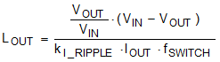
Example: VIN= 12 V, VOUT= 4.3 V, IOUT= 6 A results in an inductor value of LOUT= 2.7 µH
Once the inductor is selected, the output capacitor COUT can be determined. The value is calculated using the fact that the frequency compensation of the illumination loop has been designed for an LC-tank resonance frequency of 15 kHz:
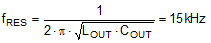
Example: COUT= 41.7 µF given that LOUT= 2.7 µH. A practical value is 2 × 22 µF. Here a parallel connection of two capacitors is chosen to lower the ESR even further.
The selected inductor and capacitor determine the output voltage ripple. The resulting output voltage ripple VLED_RIPPLE is a function of the inductor ripple kI_RIPPLE, output current IOUT, switching frequency ƒSWITCH and the capacitor value COUT:
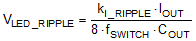
Example: kI_RIPPLE= 0.3, IOUT= 6 A, ƒSWITCH= 600 kHz and COUT= 44 µF results in an output voltage ripple of VLED_RIPPLE= 8.5 mVpp
As can be seen, this is a relative small ripple.
It is strongly advised to keep the capacitance value low. The larger the capacitor value the more energy is stored. In case of a VLED going down, stored energy needs to be dissipated. This might result in a large discharge current. For a VLED step down from V1 to V2, while the LED current was I1. The theoretical peak reverse current is:
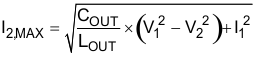
For the single-LED case, it is advised to keep COUT at maximum 44 µF.
Two other components need to be selected in the buck converter. The value of the input-capacitor (pin ILLUM_A_VIN) should be equal to or greater than the selected output capacitance COUT, in this case >44 µF. The capacitor between ILLUM_A_SWITCH and ILLUM_A_BOOST is a charge pump capacitor to drive the high side FET. The recommended value is 100 nF.