DLPS096B November 2017 – May 2022 DLPC120-Q1
PRODUCTION DATA
- 1 Features
- 2 Applications
- 3 Description
- 4 Revision History
- 5 Pin Configuration and Functions
-
6 Specifications
- 6.1 Absolute Maximum Ratings
- 6.2 ESD Ratings
- 6.3 Recommended Operating Conditions
- 6.4 Thermal Information
- 6.5 Electrical Characteristics
- 6.6 Electrical Characteristics for I/O
- 6.7 Power Supply and Reset Timing Requirements
- 6.8 Reference Clock PLL Timing Requirements
- 6.9 Parallel Interface General Timing Requirements
- 6.10 Parallel Interface Frame Timing Requirements
- 6.11 Flash Memory Interface Timing Requirements
- 6.12 DMD Interface Timing Requirements
- 6.13 JTAG Interface Timing Requirements
- 6.14 I2C Interface Timing Requirements
- 7 Parameter Measurement Information
- 8 Detailed Description
- 9 Application and Implementation
- 10Power Supply Recommendations
- 11Layout
- 12Device and Documentation Support
- 13Mechanical, Packaging, and Orderable Information
Package Options
Refer to the PDF data sheet for device specific package drawings
Mechanical Data (Package|Pins)
- ZXS|216
Thermal pad, mechanical data (Package|Pins)
Orderable Information
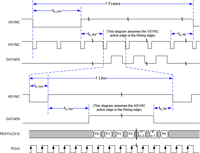
6.10 Parallel Interface Frame Timing Requirements
| MIN | MAX | UNIT | |||
|---|---|---|---|---|---|
| tp_vsw | Vertical sync width | 50% reference points | 1 | Lines | |
| tp_vbp | Vertical back porch | 50% reference points | 6 | Lines | |
| tvfp | Vertical front porch | 50% reference points | 4(1) | Lines | |
| thsw | Horizontal sync width | 50% reference points | 5 | PCLKs | |
| thbp | Horizontal back porch | 50% reference points | 4 | PCLKs | |
| thfp | Horizontal front porch | 50% reference points | 40(1) | PCLKs | |
(1) Values depend on many factors and may need to be higher depending on scaling ratio and other factors. See resolution table for typical values that have been verified.
 Figure 6-4 Parallel Interface Frame Timing