SLLSEC6E September 2012 – June 2019 DP83848-EP
PRODUCTION DATA.
- 1 Device Overview
- 2 Revision History
- 3 Pin Configuration and Functions
-
4 Specifications
- 4.1 Absolute Maximum Ratings
- 4.2 ESD Ratings
- 4.3 Recommended Operating Conditions
- 4.4 Thermal Information
- 4.5 DC Specifications
- 4.6
AC Specifications
- 4.6.1 Power Up Timing
- 4.6.2 Reset Timing
- 4.6.3 MII Serial Management Timing
- 4.6.4 100-Mbps MII Transmit Timing
- 4.6.5 100-Mbps MII Receive Timing
- 4.6.6 100BASE-TX Transmit Packet Latency Timing
- 4.6.7 100BASE-TX Transmit Packet Deassertion Timing
- 4.6.8 100BASE-TX Transmit Timing (tR/F and Jitter)
- 4.6.9 100BASE-TX Receive Packet Latency Timing
- 4.6.10 100BASE-TX Receive Packet Deassertion Timing
- 4.6.11 10-Mbps MII Transmit Timing
- 4.6.12 10-Mbps MII Receive Timing
- 4.6.13 10-Mbps Serial Mode Transmit Timing
- 4.6.14 10-Mbps Serial Mode Receive Timing
- 4.6.15 10BASE-T Transmit Timing (Start of Packet)
- 4.6.16 10BASE-T Transmit Timing (End of Packet)
- 4.6.17 10BASE-T Receive Timing (Start of Packet)
- 4.6.18 10BASE-T Receive Timing (End of Packet)
- 4.6.19 10-Mbps Heartbeat Timing
- 4.6.20 10-Mbps Jabber Timing
- 4.6.21 10BASE-T Normal Link Pulse Timing
- 4.6.22 Auto-Negotiation Fast Link Pulse (FLP) Timing
- 4.6.23 100BASE-TX Signal Detect Timing
- 4.6.24 100-Mbps Internal Loopback Timing
- 4.6.25 10-Mbps Internal Loopback Timing
- 4.6.26 RMII Transmit Timing
- 4.6.27 RMII Receive Timing
- 4.6.28 Isolation Timing
- 4.6.29 25MHz_OUT Timing
-
5 Detailed Description
- 5.1 Overview
- 5.2 Functional Block Diagram
- 5.3 Feature Description
- 5.4 Device Functional Modes
- 5.5
Programming
- 5.5.1
Architecture
- 5.5.1.1 100BASE-TX Transmitter
- 5.5.1.2
100BASE-TX Receiver
- 5.5.1.2.1 Analog Front End
- 5.5.1.2.2 Digital Signal Processor
- 5.5.1.2.3 Signal Detect
- 5.5.1.2.4 MLT-3 to NRZI Decoder
- 5.5.1.2.5 NRZI to NRZ
- 5.5.1.2.6 Serial to Parallel
- 5.5.1.2.7 Descrambler
- 5.5.1.2.8 Code-group Alignment
- 5.5.1.2.9 4B/5B Decoder
- 5.5.1.2.10 100BASE-TX Link Integrity Monitor
- 5.5.1.2.11 Bad SSD Detection
- 5.5.1.3
10BASE-T Transceiver Module
- 5.5.1.3.1 Operational Modes
- 5.5.1.3.2 Smart Squelch
- 5.5.1.3.3 Collision Detection and SQE
- 5.5.1.3.4 Carrier Sense
- 5.5.1.3.5 Normal Link Pulse Detection and Generation
- 5.5.1.3.6 Jabber Function
- 5.5.1.3.7 Automatic Link Polarity Detection and Correction
- 5.5.1.3.8 Transmit and Receive Filtering
- 5.5.1.3.9 Transmitter
- 5.5.1.3.10 Receiver
- 5.5.1
Architecture
- 5.6
Memory
- 5.6.1
Register Definition
- 5.6.1.1 Basic Mode Control Register (BMCR)
- 5.6.1.2 Basic Mode Status Register (BMSR)
- 5.6.1.3 PHY Identifier Register #1 (PHYIDR1)
- 5.6.1.4 PHY Identifier Register #2 (PHYIDR2)
- 5.6.1.5 Auto-Negotiation Advertisement Register (ANAR)
- 5.6.1.6 Auto-Negotiation Link Partner Ability Register (ANLPAR) (BASE Page)
- 5.6.1.7 Auto-Negotiation Link Partner Ability Register (ANLPAR) (Next Page)
- 5.6.1.8 Auto-Negotiate Expansion Register (ANER)
- 5.6.1.9 Auto-Negotiation Next Page Transmit Register (ANNPTR)
- 5.6.2
Extended Registers
- 5.6.2.1 PHY Status Register (PHYSTS)
- 5.6.2.2 MII Interrupt Control Register (MICR)
- 5.6.2.3 MII Interrupt Status and Miscellaneous Control Register (MISR)
- 5.6.2.4 False Carrier Sense Counter Register (FCSCR)
- 5.6.2.5 Receiver Error Counter Register (RECR)
- 5.6.2.6 100 Mbps PCS Configuration and Status Register (PCSR)
- 5.6.2.7 RMII and Bypass Register (RBR)
- 5.6.2.8 LED Direct Control Register (LEDCR)
- 5.6.2.9 PHY Control Register (PHYCR)
- 5.6.2.10 10Base-T Status/Control Register (10BTSCR)
- 5.6.2.11 CD Test and BIST Extensions Register (CDCTRL1)
- 5.6.2.12 Energy Detect Control (EDCR)
- 5.6.1
Register Definition
- 6 Application and Implementation
- 7 Power Supply Recommendations
- 8 Layout
- 9 Device and Documentation Support
- 10Mechanical, Packaging, and Orderable Information
Package Options
Mechanical Data (Package|Pins)
Thermal pad, mechanical data (Package|Pins)
Orderable Information
3 Pin Configuration and Functions
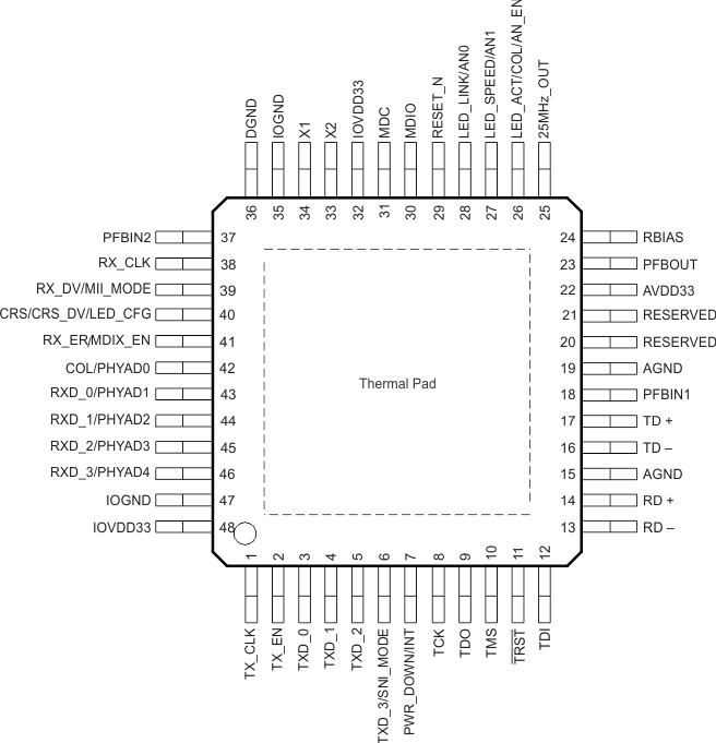
The DP83848-EP pins are classified into the following interface categories (each interface is described in the sections that follow):
- Serial management interface
- MAC data interface
- Clock interface
- LED interface
- Reset
- Strap options
- 10/100 Mbps PMD interface
- Special connect pins
- Power and ground pins
All DP83848-EP signal pins are I/O cells regardless of the particular use. The definitions below define the functionality of the I/O cells for each pin.
NOTE
Strapping pin option. See Table 3-8 for strap definitions.
- Type: IInput
- Type: OOutput
- Type: I/OInput/Output
- Type: ODOpen Drain
- Type: PD,PUInternal Pulldown/Pullup
- Type: SStrapping Pin (All strap pins have weak internal pullups or pulldowns. If the default strap value is to be changed then an external 2.2-kΩ resistor should be used. See Table 3-8 for details.)
 Figure 3-1 PHP or PTB Package (Top View)