SLVSCU7A February 2016 – March 2016 DRV10970
PRODUCTION DATA.
- 1 Features
- 2 Applications
- 3 Description
- 4 Revision History
- 5 Description (continued)
- 6 Pin Configuration and Functions
- 7 Specifications
- 8 Detailed Description
- 9 Application and Implementation
- 10Power Supply Recommendations
- 11Layout
- 12Device and Documentation Support
- 13Mechanical, Packaging, and Orderable Information
Package Options
Mechanical Data (Package|Pins)
- PWP|24
Thermal pad, mechanical data (Package|Pins)
- PWP|24
Orderable Information
9 Application and Implementation
NOTE
Information in the following applications sections is not part of the TI component specification, and TI does not warrant its accuracy or completeness. TI’s customers are responsible for determining suitability of components for their purposes. Customers should validate and test their design implementation to confirm system functionality.
9.1 Application Information
9.1.1 Hall Sensor Configuration and Connections
Hall sensors must be connected to the DRV10970 to provide the feedback of the motor position. The DRV10970 Hall sensor input circuit is capable of interfacing with a variety of Hall sensors, and with two different ways of Hall sensor placement, which are 0° placement and 30° placement.
Typically, a Hall element is used, which outputs a differential signal on the order of 100 mV or higher. The VINT regulator can be used for powering the Hall sensors, which eliminates the need for an external regulator. The Hall elements can be connected in serial or parallel as shown in Figure 21 and Figure 22.
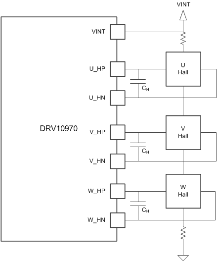 Figure 21. Serial Hall Element Connection
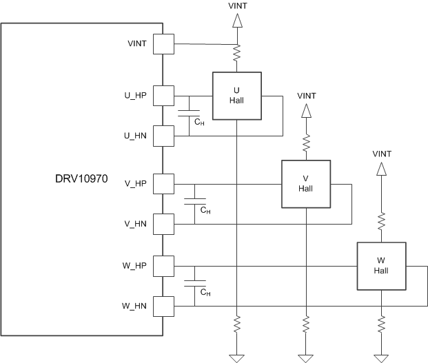 Figure 22. Parallel Hall Element Connection
Noise on the Hall signal degrades the commutation performance of the device. Therefore, take utmost care to minimize the noise while routing the Hall signals to the device inputs. The device internally has fixed time hall filtering of about 320 µs. To further minimize the high-frequency noise, a noise filtering capacitor may be connected across x_HP and x_HN pins as shown in Figure 21 andFigure 22. The value of the capacitor can be selected such that the RC time constant is in the range of 0.1 to 2 µs. For example, Hall sensor with internal impedance (between Hall output to ground) of 1 kΩ, CH value is 1 µF for 1-µs time constant.
Some motors integrate Hall sensors that provide logic outputs with open-drain type. These sensors can also be used with the DRV10970, with circuits shown in Figure 23. The negative (x_HN) inputs are biased to 2.5 V by a pair of resistors between VINT and ground. For open-drain type Hall sensors, an additional pullup resistor to supply is needed on the positive (x_HP) input, where VINT is used again. The VINT output may be used to supply power to the Hall sensors as well.
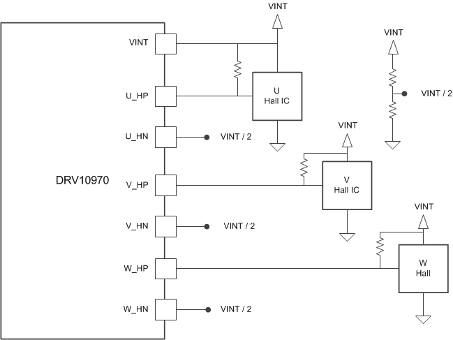 Figure 23. Hall IC Connection
The correspondence between the phase U, V, W and the Hall signal U, V, W needs to follow the DRV10970 definition, which is:
- Phase U is leading phase W by 120°, phase W is leading phase V by 120°. The Hall signal positive output is aligned with respective phase BEMF. Choose FR = 1 and 0° placement option (see Figure 24).
- Phase U is leading phase V by 120°, phase V is leading phase W by 120°. The Hall signal positive output is aligned with respective phase BEMF in the opposite direction. Choose FR = 0 and 0° placement option (see Figure 25).
- Phase U is leading phase W by 120°, phase W is leading phase V by 120°. The Hall signal positive output is 30° lagging of respective phase BEMF. Choose FR = 1 and 30° placement option (see Figure 26).
- Phase U is leading phase V by 120°, phase V is leading phase W by 120°. The Hall signal positive output is 30° leading of respective phase BEMF. Choose FR = 0 and 30° placement option (see Table 2 and Figure 29).
The correspondence and sequency is also applied to applications using open-drain output Hall ICs. Figure 28 is an example of FR = 0, and 30° placement condition.
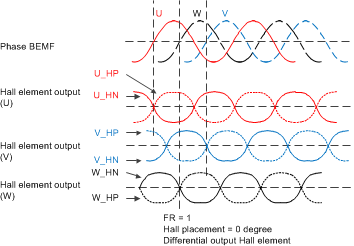 Figure 24. Correspondence Between Motor BEMF and Hall Signal
(FR = 1, 0° Placement)
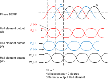 Figure 25. Correspondence Between Motor BEMF and Hall Signal
(FR = 0, 0° Placement)
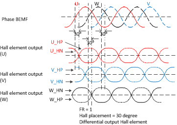 Figure 26. Correspondence Between Motor BEMF and Hall Signal
(FR = 1, 30° Placement)
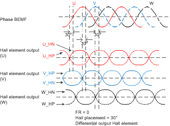 Figure 27. Correspondence Between Motor BEMF and Hall Signal
(FR = 0, 30° Placement)
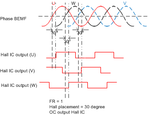 Figure 28. Correspondence Between Motor BEMF and Hall Signal
(FR = 1, 30° Placement, Hall IC)
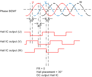 Figure 29. Correspondence Between Motor BEMF and Hall Signal
(FR = 0, 30° Placement, Hall IC)
If the motor terminal definition is different from the previous description, rename the motor phase U, V, W, or the Hall U, V, W, or swap the positive and negative of the Hall sensor output to make it match.
Use these tips to find the correct U, V, and W phases and the respective Hall sensors:
- Assume motor phases and Hall outputs do not have labels. If named, remove them.
- Label A, B, C to the motor terminals (phases). Label Da and Db, Ea and Eb, Fa and Fb to the Hall output pairs. If Hall ICs are used, just label the digital outputs as D, E, F.
- Use three 10-kΩ resistors, connect them to motor terminals - A, B, C with star connection. The center is called COM.
- Provide power to the Hall sensors.
- Use 4 channel Scope to observe signals. Connect probe -1, 2, 3 to A, B, C terminals of the motor (phases), probe-4 connects to Hall Da (or D). Name the probe 1 (terminal-A) as U-phase. (see Figure 30)
- Turn the rotor manually in clock-wise direction. If the waveform on probe-1 (U-phase) is leading probe-2 (terminal-B) by 120°, name the terminal-B as phase W and terminal-C as phase V. Else if waveform on the probe-2 is leading probe 1 (U) by 120°, terminal-B as V, terminal-C as W. At this stage all three phases of the motor are identified.
- Motor manufacturers have two popular Hall placement options. The first is 0° Hall placement (BEMF and Hall signals are in-phase) and the second is 30° Hall placement (BEMF leads Hall signal by 30°). If the probe-4 is in-phase (or lagging 30°) with phase-U, name Da as Hall U positive (U_HP), Db as Hall U negative (U_HN). If probe-4 is in-phase with phase U (or lagging 30°), but inverted polarity, name Da as U_HN, Db as U_HP. If the probe-4 is not in-phase (or lagging 30°) with respect to U but aligns with phase-V or W, name accordingly as V_HP/V_HN or W_HP/W_HN. Repeat this step to map Ea/Eb and Fa/Fb in the same way. By end of this step, all three sets of Hall signals are mapped to respective phase signals - phase U & Hall U_HP/HN, phase V & Hall V_HP/V_HN and phase W and W_HP/W_HN. Care should be taken while judging 30° Hall placement, sometimes 30° and 60° look alike. If U phase is leading Hall Da by 60°, there will be another phase (V or W) with in-phase or lagging by 30° relationship. Hence it's important to check all three phases before concluding.
- When Hall ICs are used, if the Hall D is in-phase or lagging 30° with respect to phase U but inverted polarity, name the Hall D output as U_HN, and 2.5-V reference voltage to U_HP. If Hall D is leading 30°, then turn the rotor in counter clock-wise direction and map remaining E & F Hall outputs.
- After phase UVW and Hall UVW positive negative are identified, manually rotate the motor again, check if the result matches Figure 24 and Figure 25 (0° placement) or Figure 26 and Figure 25 (30° placement).
- Connect U,V,W and Hall U,V,W to the DRV10970, with the FR = 1, it should rotate with direction you manually spun it. Connect FR = 0, the motor will spin in the other direction.
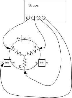 Figure 30. Motor Measurement
9.2 Typical Application
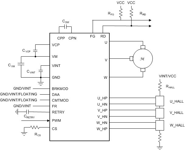 Figure 31. Typical Application Schematic
9.2.1 Design Requirements
Table 5 gives design input parameters for system design.
Table 5. Design Parameters
| DESIGN PARAMETER | EXAMPLE VALUE |
|---|---|
| Supply voltage | 5 to 18 V |
| Continuous operation current | 0 to 1 A |
| Peak current | 1.5 A |
| Hall sensor differential output peak | >40 mV |
| PWM input frequency | 15 to 100 kHz |
| PWM duty cycle | 0% to 100% |
9.2.2 Detailed Design Procedure
- Refer to Design Requirements and make sure the system meets the recommended application range.
- Refer to Hall Sensor Configuration and Connections and make sure correct phases and corresponding hall signals are identified.
- Refer to Hall Sensor Configuration and Connections and make sure hall signals are connected accurately.
- Build your hardware based on Layout Guidelines.
- Connect the device into system and validate your system.
9.2.3 Application Curves
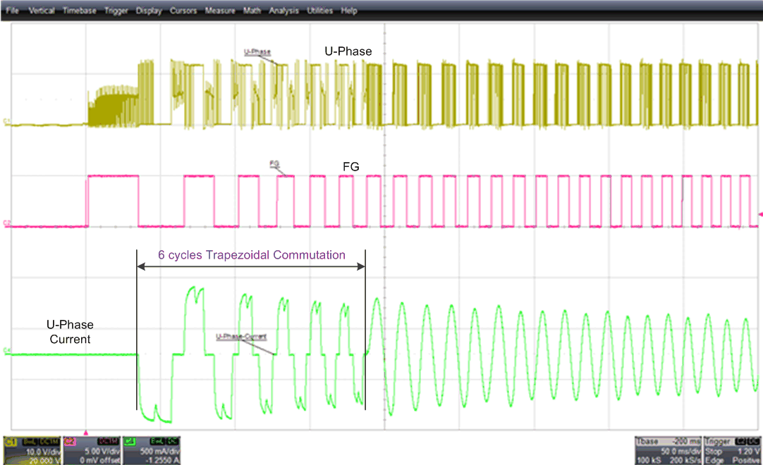 Figure 32. Three Hall Start-up Sequence
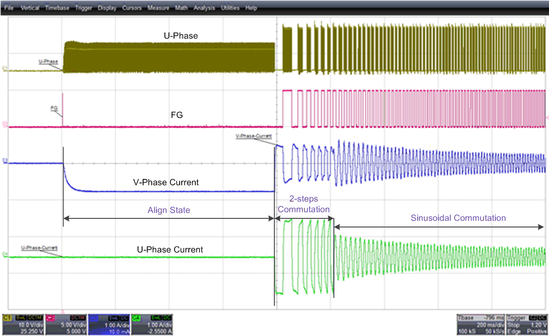 Figure 33. Single Hall Start-up Sequence