SLVSCU7A February 2016 – March 2016 DRV10970
PRODUCTION DATA.
- 1 Features
- 2 Applications
- 3 Description
- 4 Revision History
- 5 Description (continued)
- 6 Pin Configuration and Functions
- 7 Specifications
- 8 Detailed Description
- 9 Application and Implementation
- 10Power Supply Recommendations
- 11Layout
- 12Device and Documentation Support
- 13Mechanical, Packaging, and Orderable Information
Package Options
Mechanical Data (Package|Pins)
- PWP|24
Thermal pad, mechanical data (Package|Pins)
- PWP|24
Orderable Information
11 Layout
11.1 Layout Guidelines
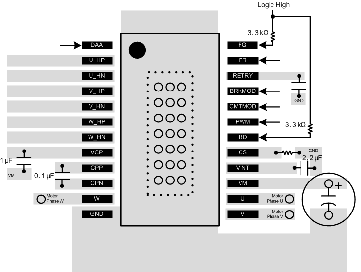
The VM terminal should be bypassed to GND using a low-ESR ceramic bypass capacitor with a recommended value of 10-µF rated for VM. Place this capacitor as close as possible to the VM pin with a thick trace or ground plane connection to the device GND pin.
The CRETRY capacitor should be placed as close to the RETRY pin as possible with a thick trace or ground plane connection to the device GND pin.
A low-ESR ceramic capacitor must be placed in between the CPN and CPP pins. TI recommends a value of 0.1-µF rated for VM. Place this component as close as possible to the pins.
A low-ESR ceramic capacitor must be placed in between the VM and VCP pins. TI recommends a value of 1-µF rated for 16 V. Place this component as close as possible to the pins.
Bypass VINT to ground with 2.2-µF ceramic capacitors rated for 10 V. Place these bypassing capacitors as close to the pins as possible.
Because the GND pin carries motor current, take utmost care while planning grounding scheme, keep the ground potential difference between any two points less than 100 mV.
11.2 Layout Example
 Figure 34. Layout Schematic