SLVSFG5D September 2020 – March 2022 DRV8300
PRODUCTION DATA
- 1 Features
- 2 Applications
- 3 Description
- 4 Revision History
- 5 Device Comparison Table
- 6 Pin Configuration and Functions
- 7 Specifications
- 8 Detailed Description
- 9 Application and Implementation
- 10Power Supply Recommendations
- 11Layout
- 12Device and Documentation Support
- 13Mechanical, Packaging, and Orderable Information
Package Options
Mechanical Data (Package|Pins)
Thermal pad, mechanical data (Package|Pins)
Orderable Information
8.3.1.2 Mode (Inverting and non inverting INLx)
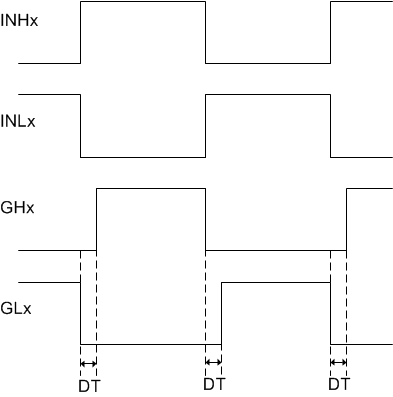
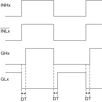
The DRV8300 has flexibility of accepting different kind of inputs on INLx. In the devices with MODE pin (QFN package), the DRV8300 provides option of configuring the GLx outputs to be inverted or non-inverted compared to polarity of signal on INLx pins. When the MODE pin is left floating, the INLx is configured to be in non-inverting mode and GLx output is in phase with respect to INLx (see Figure 8-4), whereas when the MODE pin is connected to GVDD, GLx output is out of phase with respect to INLx (see Figure 8-5). In devices without MODE pin (TSSOP package device), there are different device option available for inverting and non inverting inputs (see Section 5).
 Figure 8-4 Non-Inverted INLx inputs
 Figure 8-5 Inverted INLx inputs