SLOS842A September 2013 – June 2015 DRV8301-Q1
PRODUCTION DATA.
- 1 Features
- 2 Applications
- 3 Description
- 4 Revision History
- 5 Pin Configuration and Functions
-
6 Specifications
- 6.1 Absolute Maximum Ratings
- 6.2 ESD Ratings
- 6.3 Recommended Operating Conditions
- 6.4 Thermal Information
- 6.5 Electrical Characteristics
- 6.6 Buck Converter Characteristics
- 6.7 Current Shunt Amplifier Characteristics
- 6.8 Gate Timing and Protection Characteristics
- 6.9 SPI Timing Requirements (Slave Mode Only)
- 6.10 Typical Characteristics
- 7 Detailed Description
- 8 Application and Implementation
- 9 Power Supply Recommendations
- 10Layout
- 11Device and Documentation Support
- 12Mechanical, Packaging, and Orderable Information
Package Options
Mechanical Data (Package|Pins)
- DCA|56
Thermal pad, mechanical data (Package|Pins)
- DCA|56
Orderable Information
8 Application and Implementation
NOTE
Information in the following applications sections is not part of the TI component specification, and TI does not warrant its accuracy or completeness. TI’s customers are responsible for determining suitability of components for their purposes. Customers should validate and test their design implementation to confirm system functionality.
8.1 Application Information
The DRV8301-Q1 is a gate driver designed to drive a 3-phase BLDC motor in combination with external power MOSFETs. The device provides a high level of integration with three half-bridge gate drivers, two current shunt amplifiers, overcurrent protection, and a step-down buck regulator.
8.1.1 Gate Driver Start-up Issue Errata
The DRV8301-Q1 gate drivers may not correctly power up if a voltage greater than 8.5 V is present on any SH_X pin when EN_GATE is first brought logic high (device first enabled) after PVDD1 power is applied. This situation should be avoided by ensuring the voltage levels on the SH_X pins are less than 8.5 V when the DRV8301-Q1 is first enabled. After the first successful enable, EN_GATE can be brought low or high regardless of the SH_X pin voltage with no impact to the device operation.
8.2 Typical Application
The following design is a common application of the DRV8301-Q1.
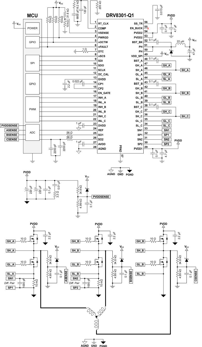 Figure 7. Typical Application Schematic
8.2.1 Design Requirements
Table 12. Design Parameters
| DESIGN PARAMETER | REFERENCE | VALUE |
|---|---|---|
| Supply voltage | PVDD | 24 V |
| Motor winding resistance | MR | 0.5 Ω |
| Motor winding inductance | ML | 0.28 mH |
| Motor poles | MP | 16 poles |
| Motor rated RPM | MRPM | 4000 RPM |
| Target full-scale current | IMAX | 14 A |
| Sense resistor | RSENSE | 0.01 Ω |
| MOSFET Qg | Qg | 29 nC |
| MOSFET RDS(on) | RDS(on) | 4.7 mΩ |
| VDS trip level | OC_ADJ_SET | 0.123 V |
| Switching frequency | ƒSW | 45 kHz |
| Series gate resistance | RGATE | 10 Ω |
| Amplifier reference | VREF | 3.3 V |
| Amplifier gain | Gain | 10 V/V |
8.2.2 Detailed Design Procedure
Table 13. Gate Driver External Components
| NAME | PIN 1 | PIN 2 | RECOMMENDED |
|---|---|---|---|
| RnOCTW | nOCTW | VCC(1) | ≥10 kΩ |
| RnFAULT | nFAULT | VCC(1) | ≥10 kΩ |
| RDTC | DTC | GND (PowerPAD) | 0 to 150 kΩ (50 ns to 500 ns) |
| CGVDD | GVDD | GND (PowerPAD) | 2.2 µF (20%) ceramic, ≥ 16 V |
| CCP | CP1 | CP2 | 0.022 µF (20%) ceramic, rated for PVDD1 |
| CDVDD | DVDD | AGND | 1 µF (20%) ceramic, ≥ 6.3 V |
| CAVDD | AVDD | AGND | 1 µF (20%) ceramic, ≥ 10 V |
| CPVDD1 | PVDD1 | GND (PowerPAD) | ≥4.7 µF (20%) ceramic, rated for PVDD1 |
| CBST_X | BST_X | SH_X | 0.1 µF (20%) ceramic, ≥ 16 V |
Table 14. Buck Regulator External Components
| NAME | PIN 1 | PIN 2 | RECOMMENDED |
|---|---|---|---|
| RRT_CLK | RT_CLK | GND (PowerPAD) | See Buck Converter |
| CCOMP | COMP | GND (PowerPAD) | See Buck Converter |
| RCCOMP | COMP | GND (PowerPAD) | See Buck Converter |
| RVSENSE1 | PH (Filtered) | VSENSE | See Buck Converter |
| RVSENSE2 | VSENSE | GND (PowerPAD) | See Buck Converter |
| RPWRGD | PWRGD | VCC(1) | ≥ 10 kΩ |
| LPH | PH | PH (Filtered) | See Buck Converter |
| DPH | PH | GND (PowerPAD) | See Buck Converter |
| CPH | PH (Filtered) | GND (PowerPAD) | See Buck Converter |
| CBST_BK | BST_BK | PH | See Buck Converter |
| CPVDD2 | PVDD2 | GND (PowerPAD) | ≥4.7 µF (20%) ceramic, rated for PVDD2 |
| CSS_TR | SS_TR | GND (PowerPAD) | See Buck Converter |
8.2.2.1 Gate Drive Average Current Load
The gate drive supply (GVDD) of the DRV8301-Q1 can deliver up to 30 mA (RMS) of current to the external power MOSFETs. Use Equation 3 to determine the approximate RMS load on the gate drive supply:
Example:
This is a rough approximation only.
8.2.2.2 Overcurrent Protection Setup
The DRV8301-Q1 provides overcurrent protection for the external power MOSFETs through the use of VDS monitors for both the high side and low side MOSFETs. These are intended for protecting the MOSFET in overcurrent conditions and not for precise current regulation.
The overcurrent protection works by monitoring the VDS voltage of the external MOSFET and comparing it against the OC_ADJ_SET register value. If the VDS exceeds the OC_ADJ_SET value the DRV8301-Q1 takes action according to the OC_MODE register.
Example:
MOSFET RDS(on) changes with temperature and this will affect the overcurrent trip level.
8.2.2.3 Sense Amplifier Setup
The DRV8301-Q1 provides two bidirectional low-side current shunt amplifiers. These can be used to sense a sum of the three half-bridges, two of the half-bridges individually, or in conjunction with an additional shunt amplifier to sense all three half-bridges individually.
- Determine the peak current that the motor will demand (IMAX). This will be dependent on the motor parameters and your specific application. I(MAX) in this example is 14 A.
- Determine the available voltage range for the current shunt amplifier. This will be ± half of the amplifier reference voltage (VREF). In this case the available range is ±1.65 V.
- Determine the sense resistor value and amplifier gain settings. There are common tradeoffs for both the sense resistor value and amplifier gain. The larger the sense resistor value, the better the resolution of the half-bridge current. This comes at the cost of additional power dissipated from the sense resistor. A larger gain value will allow you to decrease the sense resistor, but at the cost of increased noise in the output signal. This example uses a 0.01-Ω sense resistor and the minimum gain setting of the DRV8301-Q1 (10 V/V). These values allow the current shunt amplifiers to measure ±16.5 A (some additional margin on the 14 A requirement).
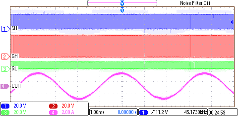
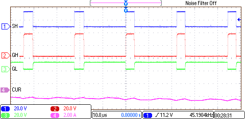
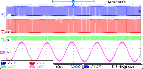
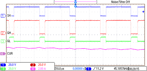
8.2.3 Application Curves
