SLOSE84B August 2022 – October 2023 DRV8452
PRODUCTION DATA
- 1
- 1 Features
- 2 Applications
- 3 Description
- 4 Revision History
- 5 Pin Configuration and Functions
- 6 Specifications
-
7 Detailed Description
- 7.1 Overview
- 7.2 Functional Block Diagram
- 7.3
Feature Description
- 7.3.1 Interface of Operation
- 7.3.2 Stepper Motor Driver Current Ratings
- 7.3.3 PWM Motor Drivers
- 7.3.4 Microstepping Indexer
- 7.3.5 Indexer Output
- 7.3.6 Automatic Microstepping Mode
- 7.3.7 Custom Microstepping Table
- 7.3.8 Current Regulation
- 7.3.9 Standstill Power Saving Mode
- 7.3.10 Current Regulation Decay Modes
- 7.3.11 Current Sensing with External Resistor
- 7.3.12 Silent step decay mode
- 7.3.13 Auto-torque Dynamic Current Adjustment
- 7.3.14 Charge Pump
- 7.3.15 Linear Voltage Regulator
- 7.3.16 VCC Voltage Supply
- 7.3.17 Logic Level, Tri-Level and Quad-Level Pin Diagrams
- 7.3.18 Spread Spectrum
- 7.3.19
Protection Circuits
- 7.3.19.1 VM Undervoltage Lockout
- 7.3.19.2 VCP Undervoltage Lockout (CPUV)
- 7.3.19.3 Logic Supply Power on Reset (POR)
- 7.3.19.4 Overcurrent Protection (OCP)
- 7.3.19.5 Stall Detection
- 7.3.19.6 Open-Load Detection (OL)
- 7.3.19.7 Overtemperature Warning (OTW)
- 7.3.19.8 Thermal Shutdown (OTSD)
- 7.3.19.9 Supply voltage sensing
- 7.3.19.10 nFAULT Output
- 7.3.19.11 Fault Condition Summary
- 7.3.20 Device Functional Modes
- 7.4 Programming
- 7.5
Register Maps
- 7.5.1 Status Registers
- 7.5.2
Control Registers
- 7.5.2.1 CTRL1 (address = 0x04) [Default = 0Fh]
- 7.5.2.2 CTRL2 (address = 0x05) [Default = 06h]
- 7.5.2.3 CTRL3 (address = 0x06) [Default = 38h]
- 7.5.2.4 CTRL4 (address = 0x07) [Default = 49h]
- 7.5.2.5 CTRL5 (address = 0x08) [Default = 03h]
- 7.5.2.6 CTRL6 (address = 0x09) [Default = 20h]
- 7.5.2.7 CTRL7 (address = 0x0A) [Default = FFh]
- 7.5.2.8 CTRL8 (address = 0x0B) [Default = 0Fh]
- 7.5.2.9 CTRL9 (address = 0x0C) [Default = 10h]
- 7.5.2.10 CTRL10 (address = 0x0D) [Default = 80h]
- 7.5.2.11 CTRL11 (address = 0x0E) [Default = FFh]
- 7.5.2.12 CTRL12 (address = 0x0F) [Default = 20h]
- 7.5.2.13 CTRL13 (address = 0x10) [Default = 10h]
- 7.5.3 Indexer Registers
- 7.5.4
Custom Microstepping Registers
- 7.5.4.1 CUSTOM_CTRL1 (address = 0x16) [Default = 00h]
- 7.5.4.2 CUSTOM_CTRL2 (address = 0x17) [Default = 00h]
- 7.5.4.3 CUSTOM_CTRL3 (address = 0x18) [Default = 00h]
- 7.5.4.4 CUSTOM_CTRL4 (address = 0x19) [Default = 00h]
- 7.5.4.5 CUSTOM_CTRL5 (address = 0x1A) [Default = 00h]
- 7.5.4.6 CUSTOM_CTRL6 (address = 0x1B) [Default = 00h]
- 7.5.4.7 CUSTOM_CTRL7 (address = 0x1C) [Default = 00h]
- 7.5.4.8 CUSTOM_CTRL8 (address = 0x1D) [Default = 00h]
- 7.5.4.9 CUSTOM_CTRL9 (address = 0x1E) [Default = 00h]
- 7.5.5
Auto torque Registers
- 7.5.5.1 ATQ_CTRL1 (address = 0x1F) [Default = 00h]
- 7.5.5.2 ATQ_CTRL2 (address = 0x20) [Default = 00h]
- 7.5.5.3 ATQ_CTRL3 (address = 0x21) [Default = 00h]
- 7.5.5.4 ATQ_CTRL4 (address = 0x22) [Default = 20h]
- 7.5.5.5 ATQ_CTRL5 (address = 0x23) [Default = 00h]
- 7.5.5.6 ATQ_CTRL6 (address = 0x24) [Default = 00h]
- 7.5.5.7 ATQ_CTRL7 (address = 0x25) [Default = 00h]
- 7.5.5.8 ATQ_CTRL8 (address = 0x26) [Default = 00h]
- 7.5.5.9 ATQ_CTRL9 (address = 0x27) [Default = 00h]
- 7.5.5.10 ATQ_CTRL10 (address = 0x28) [Default = 08h]
- 7.5.5.11 ATQ_CTRL11 (address = 0x29) [Default = 0Ah]
- 7.5.5.12 ATQ_CTRL12 (address = 0x2A) [Default = FFh]
- 7.5.5.13 ATQ_CTRL13 (address = 0x2B) [Default = 05h]
- 7.5.5.14 ATQ_CTRL14 (address = 0x2C) [Default = 0Fh]
- 7.5.5.15 ATQ_CTRL15 (address = 0x2D) [Default = 00h]
- 7.5.5.16 ATQ_CTRL16 (address = 0x2E) [Default = FFh]
- 7.5.5.17 ATQ_CTRL17 (address = 0x2F) [Default = 00h]
- 7.5.5.18 ATQ_CTRL18 (address = 0x30) [Default = 00h]
- 7.5.6 Silent Step Registers
- 8 Application and Implementation
- 9 Thermal Considerations
- 10Power Supply Recommendations
- 11Layout
- 12Device and Documentation Support
- 13Mechanical, Packaging, and Orderable Information
Package Options
Mechanical Data (Package|Pins)
Thermal pad, mechanical data (Package|Pins)
Orderable Information
7.3.6 Automatic Microstepping Mode
When the DRV8452 is operating with SPI interface, automatic microstepping mode interpolates the input step pulses to generate a current waveform corresponding to higher resolution microstep. This results in smooth sinusoidal current and noiseless operation at any step frequency.
- If automatic microstepping is disabled, the system controller will be forced to output high frequency STEP signals to generate high resolution microstepping current waveforms.
- With automatic microstepping enabled, smooth
current waveform can be generated by low frequency STEP signals.
- This drastically reduces controller overhead and is beneficial for applications such as 3D printer, factory automation and medical.
- It should be ensured that the interpolated frequency does not fall in the resonant frequency band of the stepper motor.
The EN_AUTO bit should be 1b to enable the automatic microstepping mode.
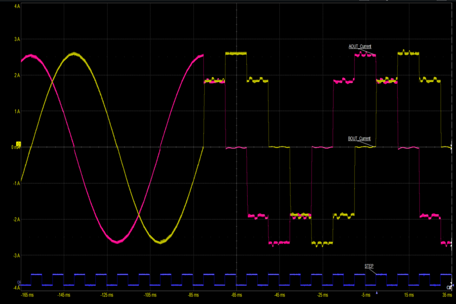
 Figure 7-7 Automatic Microstepping
Interpolation
Figure 7-7 Automatic Microstepping
InterpolationFigure 7-7 shows increment in motor angle with and without automatic microstepping. Without automatic microstepping (red plot), the motor angle increments by a large amount on every step input active edge. Automatic microstepping (green plot) results in a much smoother change in motor angle.
The DRV8452 supports interpolation to 1/32, 1/64, 1/128 or 1/256 microstepping levels, configured by the RES_AUTO bits as shown in Table 7-13. Interpolation setting can be changed on the fly.
|
RES_AUTO |
Interpolation |
|---|---|
|
00b (default) |
1/256 |
|
01b |
1/128 |
|
10b |
1/64 |
|
11b |
1/32 |
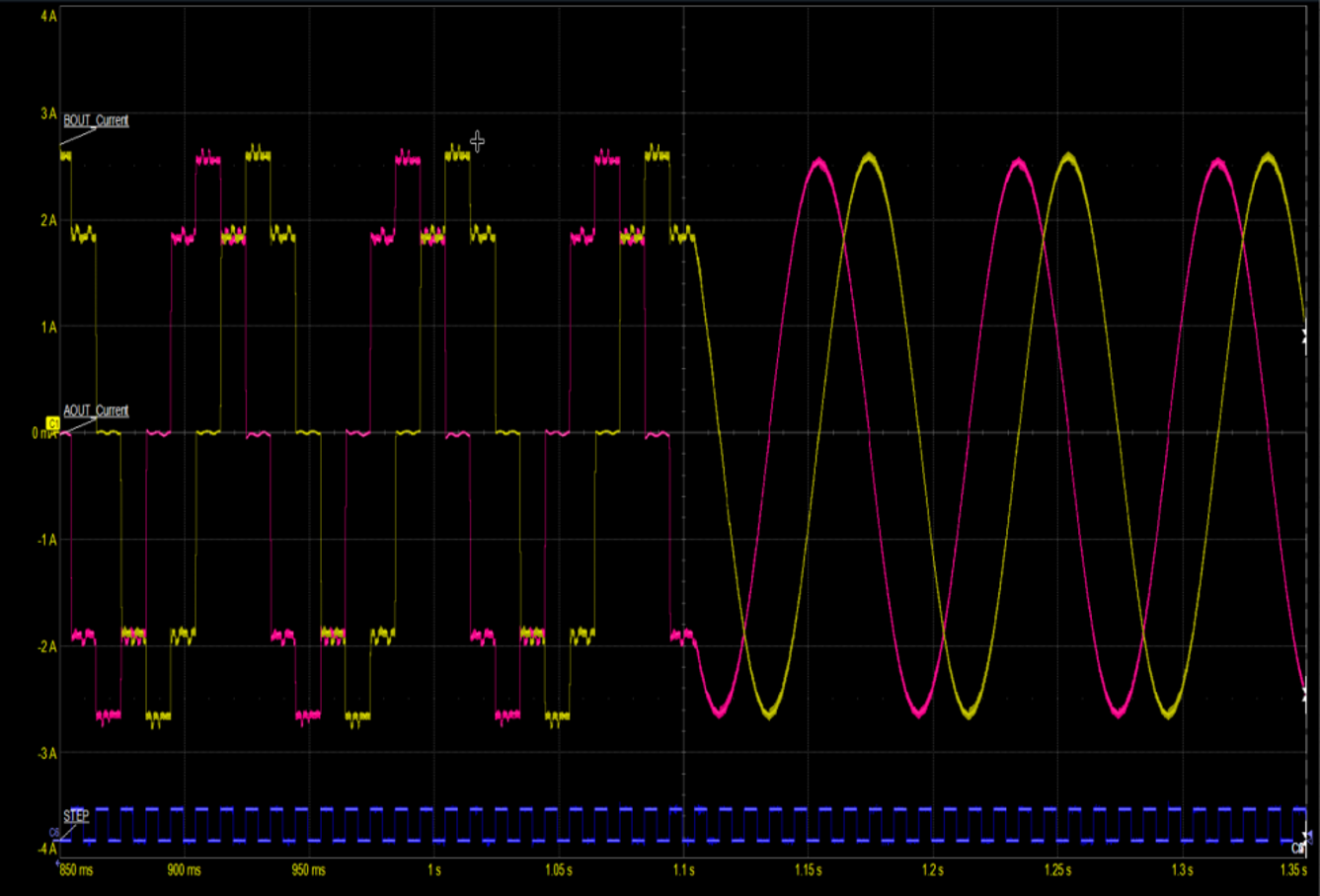
Table 7-14 show both coil currents and the smooth transition between half-step mode and automatic microstepping mode by writing 1b and 0b respectively to the EN_AUTO bit. Notice that the step frequency is same in both half-step and 1/256 automatic microstepping modes.
 |
 |
|
Transition from half-step mode to 1/256 automatic microstepping |
Transition from 1/256 automatic microstepping to half-step mode |
 Figure 7-8 Automatic Microstepping with Changing STEP Frequency
As shown in Figure 7-8, the interpolation is done based on the time between the two previous step pulses. The previous interval time is interpolated to equal divisions, depending on the RES_AUTO bit setting.
When input step frequency reduces from previous interval (shown in segment '1'), the motor holds its position till the next STEP active edge occurs. Device will go to standstill power saving mode if the EN_STSL bit is 1b, and the next active edge does not come before tSTSL_DLY expires. Standstill power saving mode is exited on the next STEP active edge.
When step frequency increases from previous interval (shown in segment '2'), the motor angle smoothly auto-corrects when the next STEP active edge comes, and the indexer moves to a position corresponding to the STEP input. In segment '3', the motor angle is incremented at a faster rate, corresponding to the step frequency of segment '2'.
The frequency of the STEP input in automatic microstepping mode should be between 10 Hz and 300 kHz.
To realize automatic microstepping for lower than 10 Hz full step equivalent step frequency, use a higher resolution microstepping setting before enabling automatic microstepping.
For example, 1 Hz step frequency in full step mode corresponds to 16 Hz step frequency in 1/16 microstepping mode. So, if one wants to use automatic microstepping for a full step 1 Hz step input, MICROSTEP_MODE can be set to 0110b (1/16 microstep), and use RES_AUTO bits for desired interpolation level.