SLOS709C June 2011 – December 2022 DRV8662
PRODUCTION DATA
- 1 Features
- 2 Applications
- 3 Description
- 4 Revision History
- 5 Pin Configuration and Functions
- 6 Specifications
- 7 Detailed Description
- 8 Application and Implementation
- 9 Power Supply Recommendations
- 10Layout
- 11Device and Documentation Support
- 12Mechanical, Packaging, and Orderable Information
Package Options
Mechanical Data (Package|Pins)
- RGP|20
Thermal pad, mechanical data (Package|Pins)
- RGP|20
Orderable Information
8.2.2.2.1 Input Filter Design
When using a PWM input, a low-pass filter is required. The primary parameters for determining the input filter are the PWM input frequency and sample rate. Because haptic waveforms are typically less than 500Hz, the input filter must attenuate frequencies above 500 Hz. For samples rates above 20 kHz, a simple first-order RC filter is recommended; however, for sample rates much lower (such as 8 kHz), a first-order filter may not sufficiently attenuate the high-frequency content. Thus, for lower sampling rates, a second-order RC filter may be required. The DRV8662EVM User's Guide contains example filter configurations for both first-order and second-order filters. The DRV8662EVM default configuration uses a second-order, differential filter, but it can be replaced by a first-order, single-ended or differential filter.
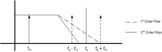
Apply these criteria to select an input filter:
- First-order RC filters, both single-ended and differential, are recommended for 20 kHz and higher data sample rates. The first-order filters have adequate settling time and the fewest components.
- Second-order filters are recommended for noiseless operation when using a lower data sample rate where a sharper cutoff is necessary.
- The attenuation at the PWM carrier frequency should be at least –40 dB for haptic applications.