SLOS709C June   2011  – December 2022 DRV8662

PRODUCTION DATA  

  1. Features
  2. Applications
  3. Description
  4. Revision History
  5. Pin Configuration and Functions
  6. Specifications
    1. 6.1 Absolute Maximum Ratings
    2. 6.2 ESD Ratings
    3. 6.3 Recommended Operating Conditions
    4. 6.4 Thermal Information
    5. 6.5 Electrical Characteristics
    6. 6.6 Timing Requirements
    7. 6.7 Typical Characteristics
  7. Detailed Description
    1. 7.1 Overview
    2. 7.2 Functional Block Diagram
    3. 7.3 Feature Description
      1. 7.3.1 Fast Start-up (Enable Pin)
      2. 7.3.2 Gain Control
      3. 7.3.3 Adjustable Boost Voltage
      4. 7.3.4 Adjustable Boost Current Limit
      5. 7.3.5 Internal Charge Pump
      6. 7.3.6 Thermal Shutdown
    4. 7.4 Device Functional Modes
      1. 7.4.1 Startup/shutdown Sequencing
        1. 7.4.1.1 PWM Source
        2. 7.4.1.2 DAC Source
      2. 7.4.2 Low-voltage Operation
    5. 7.5 Programming
      1. 7.5.1 Programming the Boost Voltage
      2. 7.5.2 Programing the Boost Current Limit
  8. Application and Implementation
    1. 8.1 Application Information
    2. 8.2 Typical Application
      1. 8.2.1 DRV8662 System Diagram with DAC Input
        1. 8.2.1.1 Design Requirements
        2. 8.2.1.2 Detailed Design Procedure
          1. 8.2.1.2.1 Inductor Selection
          2. 8.2.1.2.2 Piezo Actuator Selection
          3. 8.2.1.2.3 Boost Capacitor Selection
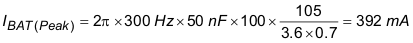
          4. 8.2.1.2.4 Current Consumption Calculation
          5. 8.2.1.2.5 Input Filter Considerations
        3. 8.2.1.3 Application Curves
      2. 8.2.2 DRV8662 System Diagram with Filtered Single-Ended PWM Input
        1. 8.2.2.1 Design Requirements
        2. 8.2.2.2 Detailed Design Procedure
          1. 8.2.2.2.1 Input Filter Design
        3. 8.2.2.3 Application Curves
  9. Power Supply Recommendations
  10. 10Layout
    1. 10.1 Layout Guidelines
    2. 10.2 Layout Example
  11. 11Device and Documentation Support
    1. 11.1 Documentation Support
      1. 11.1.1 Related Documentation
    2. 11.2 Trademarks
  12. 12Mechanical, Packaging, and Orderable Information

Package Options

Mechanical Data (Package|Pins)
Thermal pad, mechanical data (Package|Pins)
Orderable Information
Current Consumption Calculation

It is useful to understand how the voltage driven onto a piezo actuator relates to the current consumption from the power supply. Modeling a piezo element as a pure capacitor is reasonably accurate. The equation for the current through a capacitor for an applied sinusoid is given by Equation 3:

Equation 3. GUID-40C0A172-9929-406B-B20E-946454BC9866-low.gif

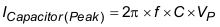
where f is the frequency of the sinusoid in Hz, C is the capacitance of the piezo load in farads, and VP is the peak voltage. At the power supply (usually a battery), the actuator current is multiplied by the boost-supply ratio and divided by the efficiency of the boost converter as shown by Equation 4.

Equation 4. GUID-7A65D0A9-14A0-4BE6-9541-3FCF6EA6DC90-low.gif

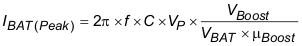
Substituting typical values for the variables of this equation yields a typical peak current seen by the battery with a sine input as in Equation 5.

Equation 5. GUID-DDEF2EAF-4181-40ED-BFEF-4C265D698DB9-low.gif