SLOS709C June   2011  – December 2022 DRV8662

PRODUCTION DATA  

  1. Features
  2. Applications
  3. Description
  4. Revision History
  5. Pin Configuration and Functions
  6. Specifications
    1. 6.1 Absolute Maximum Ratings
    2. 6.2 ESD Ratings
    3. 6.3 Recommended Operating Conditions
    4. 6.4 Thermal Information
    5. 6.5 Electrical Characteristics
    6. 6.6 Timing Requirements
    7. 6.7 Typical Characteristics
  7. Detailed Description
    1. 7.1 Overview
    2. 7.2 Functional Block Diagram
    3. 7.3 Feature Description
      1. 7.3.1 Fast Start-up (Enable Pin)
      2. 7.3.2 Gain Control
      3. 7.3.3 Adjustable Boost Voltage
      4. 7.3.4 Adjustable Boost Current Limit
      5. 7.3.5 Internal Charge Pump
      6. 7.3.6 Thermal Shutdown
    4. 7.4 Device Functional Modes
      1. 7.4.1 Startup/shutdown Sequencing
        1. 7.4.1.1 PWM Source
        2. 7.4.1.2 DAC Source
      2. 7.4.2 Low-voltage Operation
    5. 7.5 Programming
      1. 7.5.1 Programming the Boost Voltage
      2. 7.5.2 Programing the Boost Current Limit
  8. Application and Implementation
    1. 8.1 Application Information
    2. 8.2 Typical Application
      1. 8.2.1 DRV8662 System Diagram with DAC Input
        1. 8.2.1.1 Design Requirements
        2. 8.2.1.2 Detailed Design Procedure
          1. 8.2.1.2.1 Inductor Selection
          2. 8.2.1.2.2 Piezo Actuator Selection
          3. 8.2.1.2.3 Boost Capacitor Selection
          4. 8.2.1.2.4 Current Consumption Calculation
          5. 8.2.1.2.5 Input Filter Considerations
        3. 8.2.1.3 Application Curves
      2. 8.2.2 DRV8662 System Diagram with Filtered Single-Ended PWM Input
        1. 8.2.2.1 Design Requirements
        2. 8.2.2.2 Detailed Design Procedure
          1. 8.2.2.2.1 Input Filter Design
        3. 8.2.2.3 Application Curves
  9. Power Supply Recommendations
  10. 10Layout
    1. 10.1 Layout Guidelines
    2. 10.2 Layout Example
  11. 11Device and Documentation Support
    1. 11.1 Documentation Support
      1. 11.1.1 Related Documentation
    2. 11.2 Trademarks
  12. 12Mechanical, Packaging, and Orderable Information

Package Options

Mechanical Data (Package|Pins)
Thermal pad, mechanical data (Package|Pins)
Orderable Information

Description

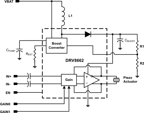
The DRV8662 is a single-chip piezo haptic driver with integrated 105 V boost switch, integrated power diode, and integrated fully-differential amplifier. This versatile device is capable of driving both high-voltage and low-voltage piezo haptic actuators. The input signal can be either differential or single-ended. The DRV8662 supports four GPIO-controlled gains: 28.8 dB, 34.8 dB, 38.4 dB, and 40.7 dB.

The boost voltage is set using two external resistors, and the boost current limit is programmable via the REXT resistor. The boost converter architecture will not allow the demand on the supply current to exceed the limit set by the REXT resistor; therefore, the DRV8662 is well-suited for portable applications. This feature also allows the user to optimize the DRV8662 circuit for a given inductor based on the desired performance requirements.

A typical start-up time of 1.5 ms makes the DRV8662 an ideal piezo driver for fast haptic responses. Thermal overload protection prevents the device from being damaged when over driven.

Device Information(1)
PART NUMBERPACKAGEBODY SIZE (NOM)
DRV8662VQFN (20)4.00 mm × 4.00 mm
For all available packages, see the orderable addendum at the end of the datasheet.
GUID-207882AB-DA2C-4EE7-A92C-5CD10FFAB4E3-low.gif Simplified Schematic