SLVSC40H June   2013  – May 2020 DRV8711

PRODUCTION DATA.  

  1. Features
  2. Applications
  3. Description
    1.     Device Images
      1.      Simplified Schematic
  4. Revision History
  5. Pin Configuration and Functions
    1.     Pin Functions
  6. Specifications
    1. 6.1 Absolute Maximum Ratings
    2. 6.2 ESD Ratings
    3. 6.3 Recommended Operating Conditions
    4. 6.4 Thermal Information
    5. 6.5 Electrical Characteristics
    6. 6.6 SPI Timing Requirements
    7. 6.7 Indexer Timing Requirements
    8. 6.8 Typical Characteristics
  7. Detailed Description
    1. 7.1 Overview
    2. 7.2 Functional Block Diagram
    3. 7.3 Feature Description
      1. 7.3.1  PWM Motor Drivers
      2. 7.3.2  Direct PWM Input Mode
      3. 7.3.3  Microstepping Indexer
      4. 7.3.4  Current Regulation
      5. 7.3.5  Decay Modes
      6. 7.3.6  Blanking Time
      7. 7.3.7  Predrivers
      8. 7.3.8  Configuring Predrivers
      9. 7.3.9  External FET Selection
      10. 7.3.10 Stall Detection
        1. 7.3.10.1 Internal Stall Detection
        2. 7.3.10.2 External Stall Detection
      11. 7.3.11 Protection Circuits
        1. 7.3.11.1 Overcurrent Protection (OCP)
        2. 7.3.11.2 Predriver Fault
        3. 7.3.11.3 Thermal Shutdown (TSD)
        4. 7.3.11.4 Undervoltage Lockout (UVLO)
    4. 7.4 Device Functional Modes
      1. 7.4.1 RESET and SLEEPn Operation
      2. 7.4.2 Microstepping Drive Current
    5. 7.5 Programming
      1. 7.5.1 Serial Data Format
    6. 7.6 Register Maps
      1. 7.6.1 Control Registers
      2. 7.6.2 CTRL Register (Address = 0x00)
      3. 7.6.3 TORQUE Register (Address = 0x01)
      4. 7.6.4 OFF Register (Address = 0x02)
      5. 7.6.5 BLANK Register (Address = 0x03)
      6. 7.6.6 DECAY Register (Address = 0x04)
      7. 7.6.7 STALL Register (Address = 0x05)
      8. 7.6.8 DRIVE Register (Address = 0x06)
      9. 7.6.9 STATUS Register (Address = 0x07)
  8. Application and Implementation
    1. 8.1 Application Information
      1. 8.1.1 Sense Resistor
      2. 8.1.2 Optional Series Gate Resistor
    2. 8.2 Typical Application
      1. 8.2.1 Design Requirements
      2. 8.2.2 Detailed Design Procedure
        1. 8.2.2.1 Set Step Rate
        2. 8.2.2.2 Calculate Current Regulation
        3. 8.2.2.3 Support External FETs
        4. 8.2.2.4 Pick Decay Mode
        5. 8.2.2.5 Config Stall Detection
        6. 8.2.2.6 Application Curves
  9. Power Supply Recommendations
    1. 9.1 Bulk Capacitance
  10. 10Layout
    1. 10.1 Layout Guidelines
    2. 10.2 Layout Example
  11. 11Device and Documentation Support
    1. 11.1 Documentation Support
      1. 11.1.1 Related Documentation
    2. 11.2 Receiving Notification of Documentation Updates
    3. 11.3 Community Resources
    4. 11.4 Trademarks
    5. 11.5 Electrostatic Discharge Caution
    6. 11.6 Glossary
  12. 12Mechanical, Packaging, and Orderable Information

Package Options

Mechanical Data (Package|Pins)
Thermal pad, mechanical data (Package|Pins)
Orderable Information

Device Images

Simplified Schematic
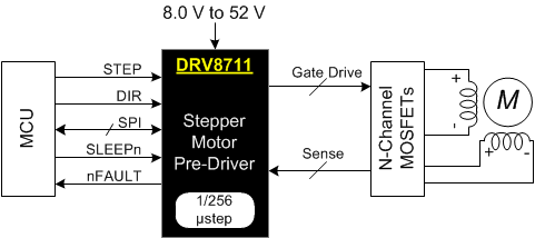
DRV8711 Simplified_SLVSC40.gif