SLVSA06K October 2009 – January 2022 DRV8824
PRODUCTION DATA
- 1 Features
- 2 Applications
- 3 Description
- 4 Revision History
- 5 Pin Configuration and Functions
- 6 Specifications
- 7 Detailed Description
- 8 Application and Implementation
- 9 Layout
- 10Device and Documentation Support
- 11Mechanical, Packaging, and Orderable Information
Package Options
Refer to the PDF data sheet for device specific package drawings
Mechanical Data (Package|Pins)
- RHD|28
- PWP|28
Thermal pad, mechanical data (Package|Pins)
Orderable Information
9.4 Power Dissipation
Power dissipation in the DRV8824 is dominated by the power dissipated in the output FET resistance, or RDS(ON). Average power dissipation when running a stepper motor can be roughly estimated by Equation 5.
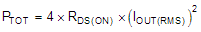
where
- PTOT is the total power dissipation
- RDS(ON) is the resistance of each FET
- IOUT(RMS) is the RMS output current being applied to each winding
IOUT(RMS) is equal to the approximately 0.7× the full-scale output current setting. The factor of 4 comes from the fact that there are two motor windings, and at any instant two FETs are conducting winding current for each winding (one high-side and one low-side).
The maximum amount of power that can be dissipated in the device is dependent on ambient temperature and heatsinking.
Note that RDS(ON) increases with temperature, so as the device heats, the power dissipation increases. This must be taken into consideration when sizing the heatsink.