SLVSA06K October   2009  – January 2022 DRV8824

PRODUCTION DATA  

  1. Features
  2. Applications
  3. Description
  4. Revision History
  5. Pin Configuration and Functions
  6. Specifications
    1. 6.1 Absolute Maximum Ratings
    2. 6.2 ESD Ratings
    3. 6.3 Recommended Operating Conditions
    4. 6.4 Thermal Information
    5. 6.5 Electrical Characteristics
    6. 6.6 Timing Requirements
    7. 6.7 Typical Characteristics
  7. Detailed Description
    1. 7.1 Overview
    2. 7.2 Functional Block Diagram
    3. 7.3 Feature Description
      1. 7.3.1 PWM Motor Drivers
      2. 7.3.2 Current Regulation
      3. 7.3.3 Decay Mode
      4. 7.3.4 Blanking Time
      5. 7.3.5 Microstepping Indexer
      6. 7.3.6 nRESET, nENBL and nSLEEP Operation
      7. 7.3.7 Protection Circuits
        1. 7.3.7.1 Overcurrent Protection (OCP)
        2. 7.3.7.2 Thermal Shutdown (TSD)
        3. 7.3.7.3 Undervoltage Lockout (UVLO)
    4. 7.4 Device Functional Modes
      1. 7.4.1 STEP/DIR Interface
      2. 7.4.2 Microstepping
  8. Application and Implementation
    1. 8.1 Application Information
    2. 8.2 Typical Application
      1. 8.2.1 Design Requirements
      2. 8.2.2 Detailed Design Procedure
        1. 8.2.2.1 Stepper Motor Speed
        2. 8.2.2.2 Current Regulation
        3. 8.2.2.3 Decay Modes
      3. 8.2.3 Application Curves
  9. Layout
    1. 9.1 Layout Guidelines
    2. 9.2 Layout Example
    3. 9.3 Thermal Considerations
    4. 9.4 Power Dissipation
    5. 9.5 Heatsinking
  10. 10Device and Documentation Support
    1. 10.1 Community Resources
    2. 10.2 Trademarks
  11. 11Mechanical, Packaging, and Orderable Information

Package Options

Refer to the PDF data sheet for device specific package drawings

Mechanical Data (Package|Pins)
  • RHD|28
  • PWP|28
Thermal pad, mechanical data (Package|Pins)
Orderable Information

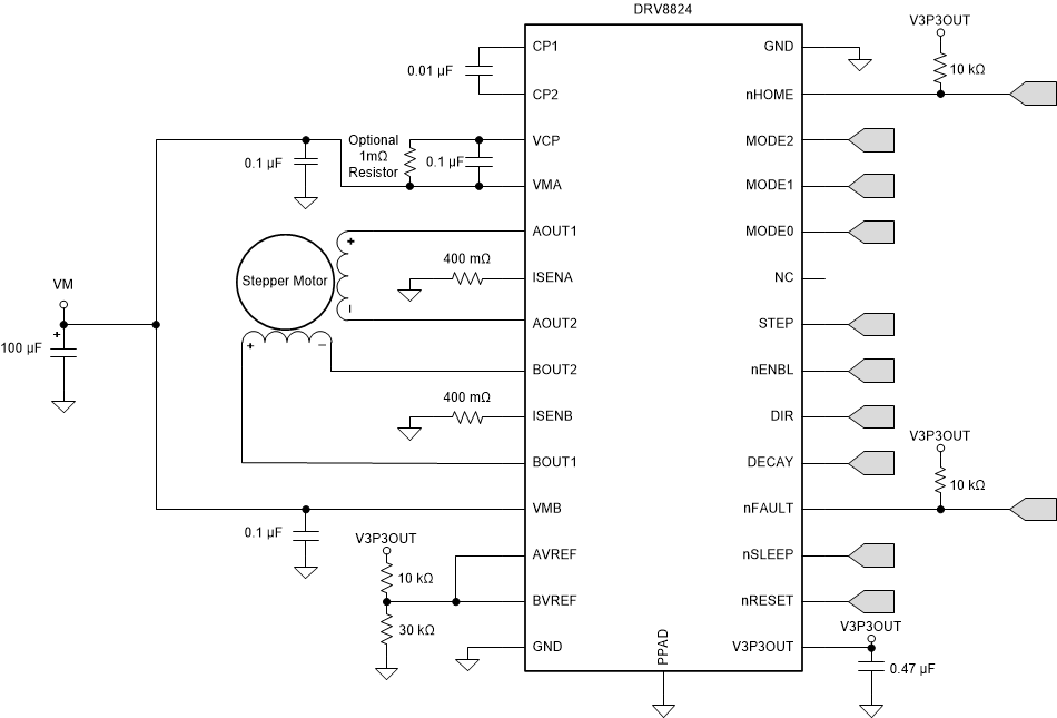
Typical Application

GUID-2E21DDBC-658D-4CE4-B34D-F20E00587F02-low.gifFigure 8-1 Typical Application Diagram