SLLSEK2A June 2014 – March 2017 DRV8846
PRODUCTION DATA.
- 1 Features
- 2 Applications
- 3 Description
- 4 Revision History
- 5 Pin Configuration and Functions
- 6 Specifications
- 7 Detailed Description
- 8 Application and Implementation
- 9 Power Supply Recommendations
- 10Layout
- 11Device and Documentation Support
- 12Mechanical, Packaging, and Orderable Information
Package Options
Mechanical Data (Package|Pins)
- RGE|24
Thermal pad, mechanical data (Package|Pins)
- RGE|24
Orderable Information
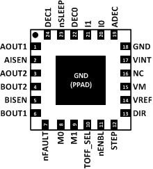
5 Pin Configuration and Functions
RGE Package
24-Pin VQFN With Exposed Thermal PAD
Top View

Pin Functions
| PIN | I/O | DESCRIPTION | ||
|---|---|---|---|---|
| NAME | NO. | |||
| ADEC | 19 | I | Smart tune enable | Logic low sets decay modes by DEC0 and DEC1 pins; logic high – smart tune operation is enabled; must be set prior to coming out of sleep; internal pulldown |
| AISEN | 2 | O | Winding A sense | Connect to current sense resistor for bridge A, or GND if current regulation is not required |
| AOUT1 | 1 | O | Winding A output | |
| AOUT2 | 3 | |||
| BISEN | 5 | O | Winding B sense | Connect to current sense resistor for bridge B, or GND if current regulation is not required |
| BOUT1 | 6 | O | Winding B output | |
| BOUT2 | 4 | |||
| DEC0 | 22 | I | Decay mode setting pins | Sets the decay mode; see description section; tri-level pin |
| DEC1 | 24 | I | ||
| DIR | 13 | I | Direction input | Logic level sets the direction of stepping; internal pulldown |
| GND | 18, PPAD | PWR | Device ground | Both the GND pin and device thermal pad must be connected to ground |
| I0 | 20 | I | Torque DAC current scalar | Scales the current from 100% to 12.5% in 12.5% steps; tri-level pin |
| I1 | 21 | I | ||
| MO | 8 | I | Microstepping mode setting pins | Controls step mode (full, half, up to 1/32-step) and single- or dual-edge clocking; tri-level pin |
| M1 | 9 | I | ||
| NC | 16 | — | No connect | Unused pin not connected internally |
| nENBL | 11 | I | Enable driver output | Logic low to enable device outputs and internal indexer; logic high to disable; internal pulldown |
| nFAULT | 7 | OD | Fault indication pin | Pulled logic low with fault condition; open-drain output requires external pullup |
| nSLEEP | 23 | I | Sleep mode input | Logic high to enable device; logic low to enter low-power sleep mode; internal pulldown |
| STEP | 12 | I | Step input | A rising edge (or rising and falling depending on step mode) advances the indexer one step; internal pulldown |
| TOFF_SEL | 10 | I | Decay mode off time set | Sets the off-time during current chopping; tri-level pin |
| VINT | 17 | — | Internal regulator | Internal supply voltage; bypass to GND with 2.2-μF, 6.3-V capacitor |
| VM | 15 | PWR | Power supply | Connect to motor power supply; bypass to GND with a 0.1- and 10-μF (minimum) ceramic capacitor rated for VM |
| VREF | 14 | I | Full-scale current reference input | Voltage on this pin sets the full scale chopping current; short to VINT if not supplying an external reference voltage |