SLVSEC9C September 2019 – February 2020 DRV8904-Q1 , DRV8906-Q1 , DRV8908-Q1 , DRV8910-Q1 , DRV8912-Q1
PRODUCTION DATA.
- 1 Features
- 2 Applications
- 3 Description
- 4 Revision History
- 5 Device Comparison Table
- 6 Pin Configuration and Functions
- 7 Specifications
-
8 Detailed Description
- 8.1 Overview
- 8.2 Functional Block Diagram
- 8.3
Feature Description
- 8.3.1
Half Bridge Drivers
- 8.3.1.1
Control Modes
- 8.3.1.1.1 Continuous Mode (Without PWM)
- 8.3.1.1.2 Chopping Mode (With PWM)
- 8.3.1.1.3 Parallel Mode (Continuous Operation)
- 8.3.1.1.4
Parallel Mode (PWM Operation)
- 8.3.1.1.4.1 PWM Configuration
- 8.3.1.1.4.2 Free-Wheeling Mode (Synchronous Rectification) Disable / Enable
- 8.3.1.1.4.3 PWM Channels Mapping
- 8.3.1.1.4.4 PWM Channels Configuration (PWM Frequency and PWM Duty)
- 8.3.1.1.4.5 PWM Generators Disable
- 8.3.1.1.4.6 Half-Bridge Enable
- 8.3.1.1.4.7 PWM Generators Enable
- 8.3.1.2 Half-Bridge Drive Architecture
- 8.3.1.1
Control Modes
- 8.3.2 Pin Diagrams
- 8.3.3 Protection Circuits
- 8.3.1
Half Bridge Drivers
- 8.4 Device Functional Modes
- 8.5 Programming
- 8.6
Register Map
- 8.6.1
DRV8912-Q1 and DRV8910-Q1 Register Maps
- 8.6.1.1
Status Registers
- 8.6.1.1.1 IC Status (IC_STAT) Register (Address = 0x00) [reset = 0x00]
- 8.6.1.1.2 Overcurrent Protection (OCP) Status 1 (OCP_STAT_1) Register (Address = 0x01) [reset = 0x00]
- 8.6.1.1.3 Overcurrent Protection (OCP) Status 2 (OCP_STAT_2) Register (Address = 0x02) [reset = 0x00]
- 8.6.1.1.4 Overcurrent Protection (OCP) Status 3 (OCP_STAT_3) Register (Address = 0x03) [reset = 0x00]
- 8.6.1.1.5 Open-Load Detect (OLD) Status 1 (OLD_STAT_1) Register (Address = 0x04) [reset = 0x00]
- 8.6.1.1.6 Open-Load Detect (OLD) Status 2 (OLD_STAT_2) Register (Address = 0x05) [reset = 0x00]
- 8.6.1.1.7 Open-Load Detect (OLD) Status 3 (OLD_STAT_3) Register (Address = 0x06) [reset = 0x00]
- 8.6.1.2
Control Registers
- 8.6.1.2.1 Configuration (CONFIG_CTRL) Register (Address = 0x07) [reset = 0x00]
- 8.6.1.2.2 Operation Control 1 (OP_CTRL_1) Register (Address = 0x08) [reset = 0x00]
- 8.6.1.2.3 Operation Control 2 (OP_CTRL_2) Register (Address = 0x09) [reset = 0x00]
- 8.6.1.2.4 Operation Control 3 (OP_CTRL_3) Register (Address = 0x0A) [reset = 0x00]
- 8.6.1.2.5 PWM Control 1 (PWM_CTRL_1) Register (Address = 0x0B) [reset = 0x00]
- 8.6.1.2.6 PWM Control 2 (PWM_CTRL_2) Register (Address = 0x0C) [reset = 0x00]
- 8.6.1.2.7 Free-Wheeling Control 1 (FW_CTRL_1) Register (Address = 0x0D) [reset = 0x00]
- 8.6.1.2.8 Free-Wheeling Control 2 (FW_CTRL_2) Register (Address = 0x0E) [reset = 0x00]
- 8.6.1.2.9 PWM Map Control 1 (PWM_MAP_CTRL_1) Register (Address = 0x0F) [reset = 0x00]
- 8.6.1.2.10 PWM Map Control 2 (PWM_MAP_CTRL_2) Register (Address = 0x10) [reset = 0x00]
- 8.6.1.2.11 PWM Map Control 3 (PWM_MAP_CTRL_3) Register (Address = 0x11) [reset = 0x00]
- 8.6.1.2.12 PWM Frequency Control (PWM_FREQ_CTRL) Register (Address = 0x12) [reset = 0x00]
- 8.6.1.2.13 PWM Duty Control Channel 1 (PWM_DUTY_CH1) Register (Address = 0x13) [reset = 0x00]
- 8.6.1.2.14 PWM Duty Control Channel 2 (PWM_DUTY_CH2) Register (Address = 0x14) [reset = 0x00]
- 8.6.1.2.15 PWM Duty Control Channel 3 (PWM_DUTY_CH3) Register (Address = 0x15) [reset = 0x00]
- 8.6.1.2.16 PWM Duty Control Channel 4 (PWM_DUTY_CH4) Register (Address = 0x16) [reset = 0x00]
- 8.6.1.2.17 Slew Rate Control 1 (SR_CTRL_1) Register (Address = 0x17) [reset = 0x00]
- 8.6.1.2.18 Slew Rate Control 2 (SR_CTRL_2) Register (Address = 0x18) [reset = 0x00]
- 8.6.1.2.19 Open-Load Detect (OLD) Control 1 (OLD_CTRL_1) Register (Address = 0x19) [reset = 0x00]
- 8.6.1.2.20 Open-Load Detect (OLD) Control 2 (OLD_CTRL_2) Register (Address = 0x1A) [reset = 0x00]
- 8.6.1.2.21 Open-Load Detect (OLD) Control 3 (OLD_CTRL_3) Register (Address = 0x1B) [reset = 0x00]
- 8.6.1.2.22 Open-Load Detect (OLD) Control 4 (OLD_CTRL_4) Register (Address = 0x24) [reset = 0x00]
- 8.6.1.1
Status Registers
- 8.6.2
DRV8908-Q1, DRV8906-Q1 and DRV8904-Q1 Register Maps
- 8.6.2.1
Status Registers
- 8.6.2.1.1 IC Status (IC_STAT) Register (Address = 0x00) [reset = 0x00]
- 8.6.2.1.2 Overcurrent Protection (OCP) Status 1 (OCP_STAT_1) Register (Address = 0x01) [reset = 0x00]
- 8.6.2.1.3 Overcurrent Protection (OCP) Status 2 (OCP_STAT_2) Register (Address = 0x02) [reset = 0x00]
- 8.6.2.1.4 Overcurrent Protection (OCP) Status 3 (OCP_STAT_3) Register (Address = 0x03) [reset = 0x00]
- 8.6.2.1.5 Open-Load Detect (OLD) Status 1 (OLD_STAT_1) Register (Address = 0x04) [reset = 0x00]
- 8.6.2.1.6 Open-Load Detect (OLD) Status 2 (OLD_STAT_2) Register (Address = 0x05) [reset = 0x00]
- 8.6.2.1.7 Open-Load Detect (OLD) Status 3 (OLD_STAT_3) Register (Address = 0x06) [reset = 0x00]
- 8.6.2.2
Control Registers
- 8.6.2.2.1 Configuration (CONFIG_CTRL) Register (Address = 0x07) [reset = 0x00]
- 8.6.2.2.2 Operation Control 1 (OP_CTRL_1) Register (Address = 0x08) [reset = 0x00]
- 8.6.2.2.3 Operation Control 2 (OP_CTRL_2) Register (Address = 0x09) [reset = 0x00]
- 8.6.2.2.4 Operation Control 3 (OP_CTRL_3) Register (Address = 0x0A) [reset = 0x00]
- 8.6.2.2.5 PWM Control 1 (PWM_CTRL_1) Register (Address = 0x0B) [reset = 0x00]
- 8.6.2.2.6 PWM Control 2 (PWM_CTRL_2) Register (Address = 0x0C) [reset = 0x00]
- 8.6.2.2.7 Free-Wheeling Control 1 (FW_CTRL_1) Register (Address = 0x0D) [reset = 0x00]
- 8.6.2.2.8 Free-Wheeling Control 2 (FW_CTRL_2) Register (Address = 0x0E) [reset = 0x00]
- 8.6.2.2.9 PWM Map Control 1 (PWM_MAP_CTRL_1) Register (Address = 0x0F) [reset = 0x00]
- 8.6.2.2.10 PWM Map Control 2 (PWM_MAP_CTRL_2) Register (Address = 0x10) [reset = 0x00]
- 8.6.2.2.11 PWM Map Control 3 (PWM_MAP_CTRL_3) Register (Address = 0x11) [reset = 0x00]
- 8.6.2.2.12 PWM Map Control 4 (PWM_MAP_CTRL_4) Register (Address = 0x12) [reset = 0x00]
- 8.6.2.2.13 PWM Frequency Control 1 (PWM_FREQ_CTRL_1) Register (Address = 0x13 [reset = 0x00]
- 8.6.2.2.14 PWM Frequency Control 2 (PWM_FREQ_CTRL_2) Register (Address = 0x14 [reset = 0x00]
- 8.6.2.2.15 PWM Duty Control Channel 1 (PWM_DUTY_CH1) Register (Address = 0x15) [reset = 0x00]
- 8.6.2.2.16 PWM Duty Control Channel 2 (PWM_DUTY_CH2) Register (Address = 0x16) [reset = 0x00]
- 8.6.2.2.17 PWM Duty Control Channel 3 (PWM_DUTY_CH3) Register (Address = 0x17) [reset = 0x00]
- 8.6.2.2.18 PWM Duty Control Channel 4 (PWM_DUTY_CH4) Register (Address = 0x18) [reset = 0x00]
- 8.6.2.2.19 PWM Duty Control Channel 5 (PWM_DUTY_CH5) Register (Address = 0x19) [reset = 0x00]
- 8.6.2.2.20 PWM Duty Control Channel 6 (PWM_DUTY_CH6) Register (Address = 0x1A) [reset = 0x00]
- 8.6.2.2.21 PWM Duty Control Channel 7 (PWM_DUTY_CH7) Register (Address = 0x1B) [reset = 0x00]
- 8.6.2.2.22 PWM Duty Control Channel 8 (PWM_DUTY_CH8) Register (Address = 0x1C) [reset = 0x00]
- 8.6.2.2.23 Slew Rate Control 1 (SR_CTRL_1) Register (Address = 0x1D [reset = 0x00]
- 8.6.2.2.24 Slew Rate Control 2 (SR_CTRL_2) Register (Address = 0x1E) [reset = 0x00]
- 8.6.2.2.25 Open-Load Detect (OLD) Control 1 (OLD_CTRL_1) Register (Address = 0x1F) [reset = 0x00]
- 8.6.2.2.26 Open-Load Detect (OLD) Control 2 (OLD_CTRL_2) Register (Address = 0x20) [reset = 0x00]
- 8.6.2.2.27 Open-Load Detect (OLD) Control 3 (OLD_CTRL_3) Register (Address = 0x21) [reset = 0x00]
- 8.6.2.2.28 Open Load Detect (OLD) Control 4 (OLD_CTRL_4) Register (Address = 0x22) [reset = 0x00]
- 8.6.2.2.29 Open Load Detect (OLD) Control 5 (OLD_CTRL_5) Register (Address = 0x23) [reset = 0x00]
- 8.6.2.2.30 Open Load Detect (OLD) Control 6 (OLD_CTRL_6) Register (Address = 0x24) [reset = 0x00]
- 8.6.2.1
Status Registers
- 8.6.1
DRV8912-Q1 and DRV8910-Q1 Register Maps
- 9 Application and Implementation
- 10Power Supply Recommendations
- 11Layout
- 12Device and Documentation Support
- 13Mechanical, Packaging, and Orderable Information
Package Options
Mechanical Data (Package|Pins)
- PWP|24
Thermal pad, mechanical data (Package|Pins)
- PWP|24
Orderable Information
9.3.3 Thermal Parameters
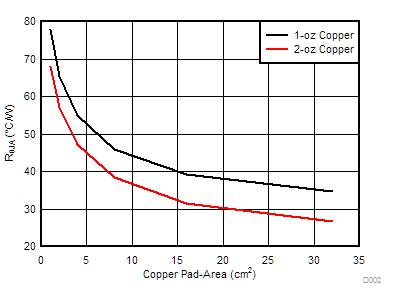
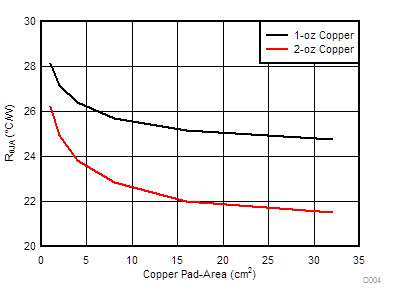
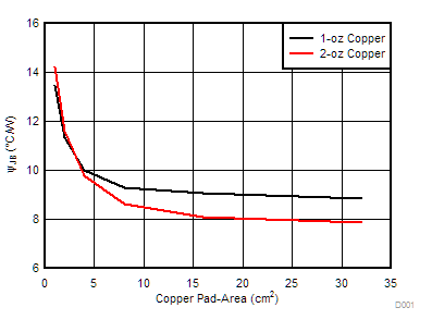
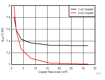
The variation of thermal parameters such as the RθJA (Junction-to-Ambient Thermal Resistance) and ΨJB (Junction-to-Board Characterization Parameter) is highly dependent on the PCB type, copper thickness and the copper pad area.
Figure 152 and Figure 153 shows the variation of the RθJA (Junction-to-Ambient Thermal Resistance) and ΨJB (Junction-to-Board Characterization Parameter) with copper-pad area for 2-layer PCB. As shown in these curves, the thermal resistance is lower for the higher copper thickness PCB and the higher copper pad-area.
Similarly, Figure 154 and Figure 153 shows the variation of the RθJA and ΨJB with copper-pad area for 4-layer PCB respectively.
NOTE
The thermal parameters (RθJA (Junction-to-Ambient Thermal Resistance) and ΨJB (Junction-to-Board Characterization Parameter)) are calculated considering the ambient temperature of 25°C and with 1.5-W power evenly dissipated between high-side and low-side FET's. The thermal parameters calculated considering the power dissipation at the actual location of the power-FETs rather than an averaged estimation.
The thermal parameters are highly dependent on the external conditions such as altitude, package geometry etc. Refer to Application Report for more details.
 Figure 152. 2-Layer PCB Junction-to-Ambient Thermal Resistance (RθJA) vs Copper Area
  Figure 154. 4-Layer PCB Junction-to-Ambient Thermal Resistance (RθJA) vs Copper Area
  Figure 153. 2-Layer PCB Junction-to-Board Characterization Parameter (ΨJB) vs Copper Area
  Figure 155. 4-Layer PCB Junction-to-Board Characterization (ΨJB) Parameter vs Copper Area