SNLS658 December 2020 DS160PR810
PRODUCTION DATA
- 1 Features
- 2 Applications
- 3 Description
- 4 Revision History
- 5 Pin Configuration and Functions
- 6 Specifications
- 7 Detailed Description
- 8 Application and Implementation
- 9 Power Supply Recommendations
- 10Layout
- 11Device and Documentation Support
- 12Mechanical, Packaging, and Orderable Information
Package Options
Mechanical Data (Package|Pins)
- NJX|64
Thermal pad, mechanical data (Package|Pins)
Orderable Information
8.2.1.2 Detailed Design Procedure
In PCIe Gen 4.0 and Gen 3.0 applications, the specification requires Rx-Tx (of root-complex and endpoint) link training to establish and optimize signal conditioning settings at 16 Gbps and 8 Gbps, respectively. In link training, the Rx partner requests a series of FIR – preshoot and deemphasis coefficients (10 Presets) from the Tx partner. The Rx partner includes 7-levels (6 dB to 12 dB) of CTLE followed by a single tap DFE. The link training would pre-condition the signal, with an equalized link between the root-complex and endpoint resulting an optimized link. Note that there is no link training in PCIe Gen 1.0 (2.5 Gbps) or PCIe Gen 2.0 (5.0 Gbps) applications.
For operation in PCIe 4.0 or 3.0 links, the DS160PR810 is designed with linear datapth to pass the Tx preset signaling (by root complex and end point) onto the Rx (of root complex and end point) to train and optimize the equalization settings. The linear redriver device helps extend the PCB trace reach distance by boosting the attenuated signals with its equalization, which allows the user to recover the signal by the downstream Rx more easily. The device must be placed in between the Tx and Rx (of root complex and end point) such a way that both RX and TX signal swing stays within the linearity range of the device. Adjustments to the device EQ setting should be performed based on the channel loss to optimize the eye opening in the Rx partner. The available EQ gain settings are provided in Table 7-1. For most PCIe systems the default DC gain setting GAIN = floating would be sufficient.
The DS160PR810 can be optimized for a given system utlizing its three configuration modes - Pin Mode, SMBus/I2C Master Mode and SMBus/I2C Slave Mode. In SMBus/I2C modes the SCL, SDA pins must be pulled up to a 3.3 V supply with a pull-up resistor. The value of the resistor depends on total bus capacitance. 4.7 kΩ is a good first approximation for a bus capacitance of 10 pF.
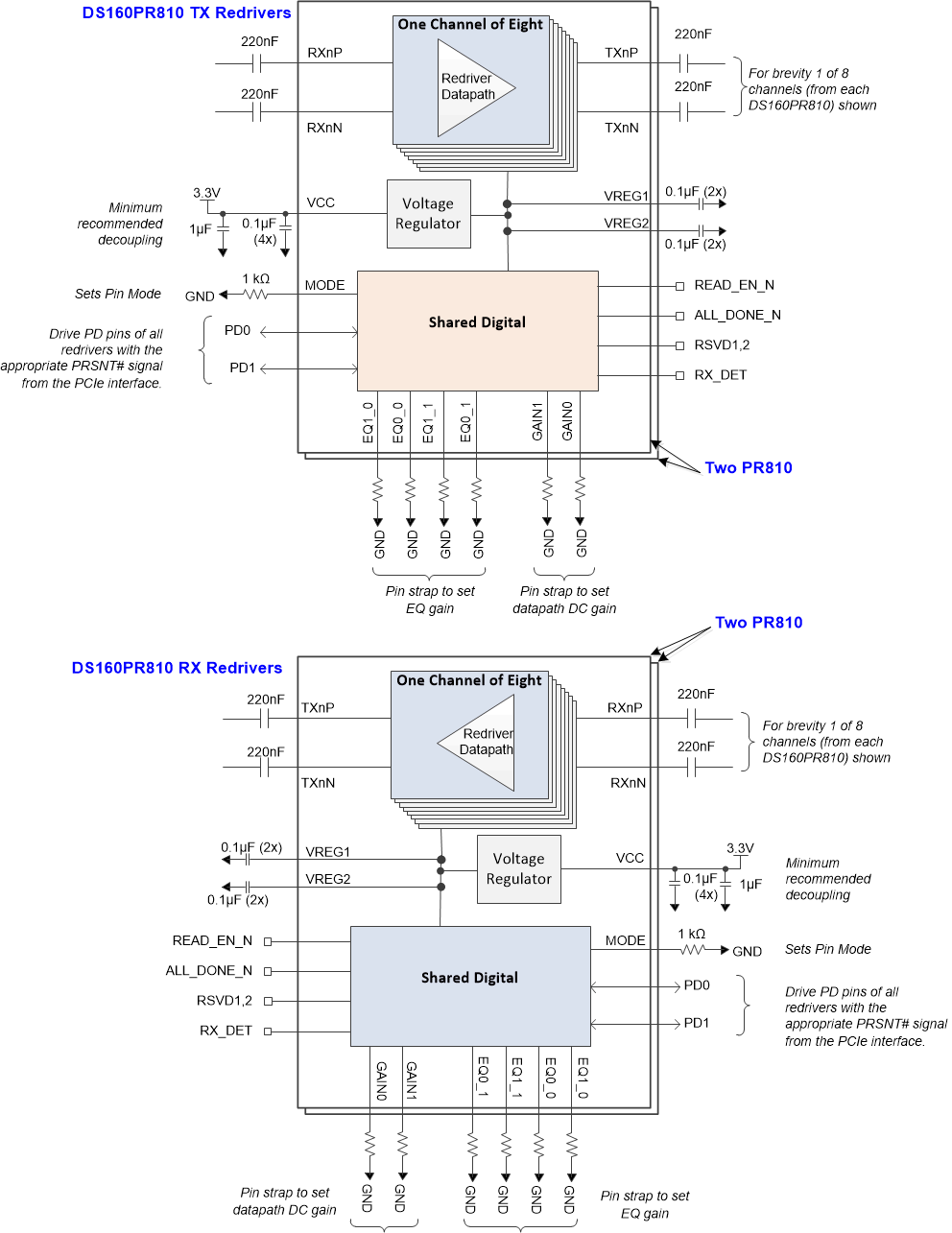
Figure 8-2 shows a simplified schematic for x16lane configuration in Pin Mode.
 Figure 8-2 Simplified Schematic for PCIe
x16 Lane Configuration in Pin Mode
Figure 8-2 Simplified Schematic for PCIe
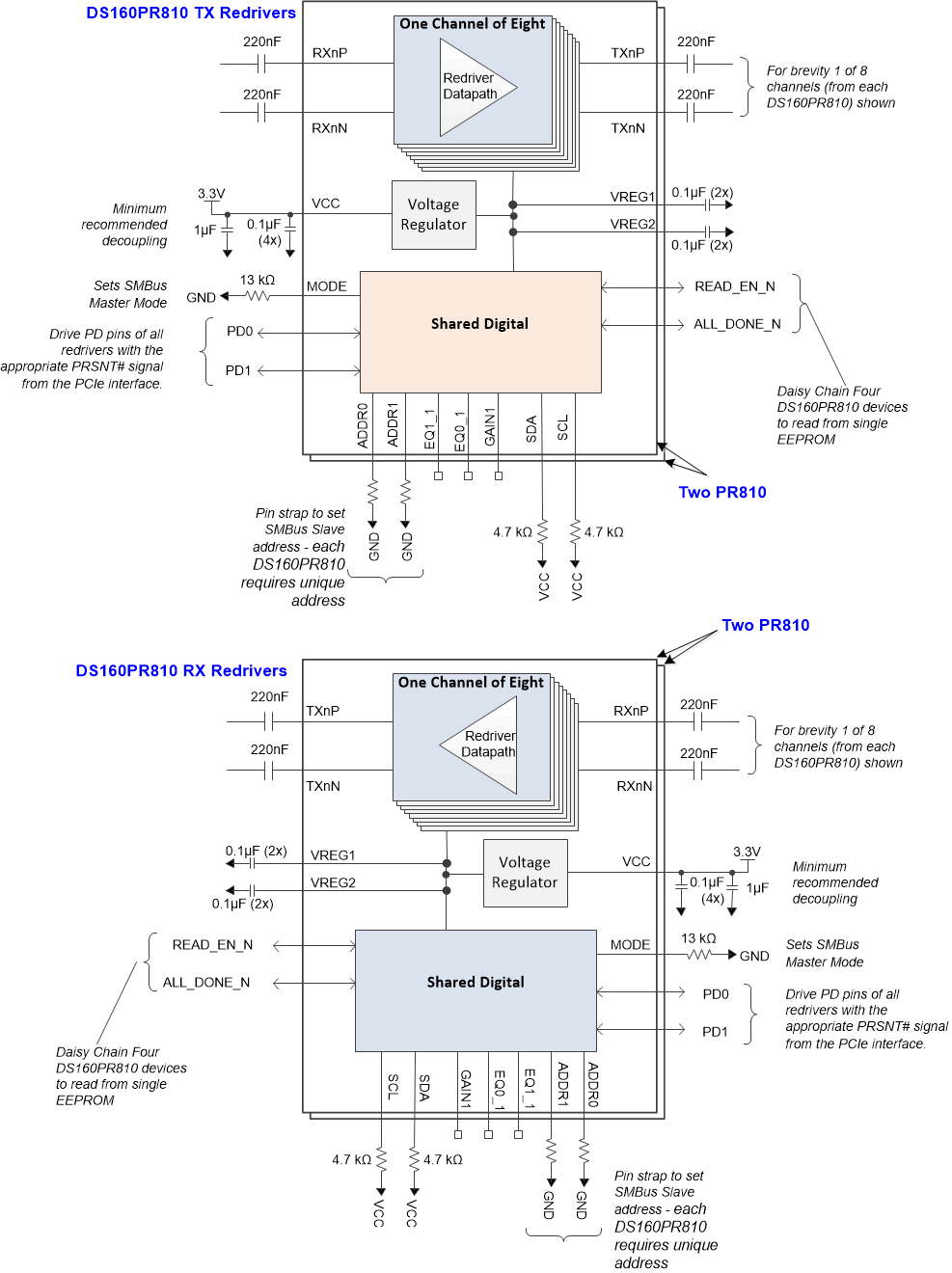
x16 Lane Configuration in Pin ModeFigure 8-3 shows a simplified schematic for PCIe x16 lane configuration in SMBus/I2C Master Mode.
 Figure 8-3 Simplified Schematic for PCIe x16
Lane
Configuration in SMBus/I2C Master Mode
Figure 8-3 Simplified Schematic for PCIe x16
Lane
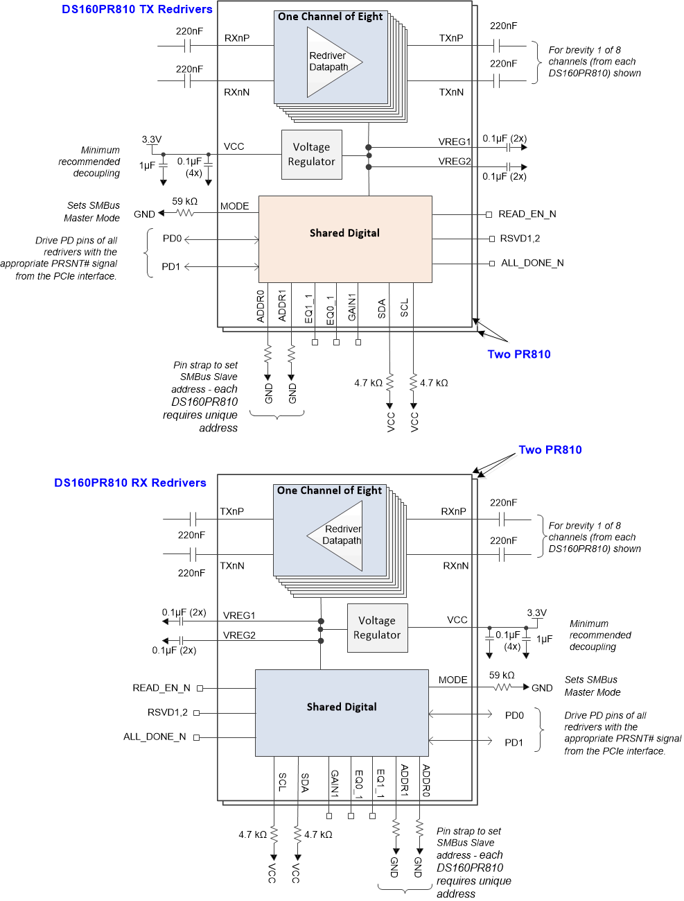
Configuration in SMBus/I2C Master ModeFigure 8-4 shows a simplified schematic for x16 lane configuration in SMBus/I2C Slave Mode.
 Figure 8-4 Simplified Schematic for PCIe
x16 Lane Configuration in
SMBus/I2C Slave Mode