SNLS244H September 2006 – January 2016 DS42MB100
PRODUCTION DATA.
- 1 Features
- 2 Applications
- 3 Description
- 4 Revision History
- 5 Pin Configuration and Functions
- 6 Specifications
- 7 Parameter Measurement Information
- 8 Detailed Description
- 9 Application and Implementation
- 10Power Supply Recommendations
- 11Layout
- 12Device and Documentation Support
- 13Mechanical, Packaging, and Orderable Information
Package Options
Refer to the PDF data sheet for device specific package drawings
Mechanical Data (Package|Pins)
- NJK|36
Thermal pad, mechanical data (Package|Pins)
Orderable Information
11 Layout
11.1 Layout Guidelines
Use at least a four layer board with a power and ground plane. Closely-coupled differential lines of 100 Ω are typically recommended for differential interconnect. The closely coupled lines help to ensure that coupled noise will appear as common-mode and thus will be rejected by the receivers. Information on the WQFN style package is provided in AN-1187 Leadless Leadframe Package (LLP), SNOA401.
11.2 Layout Example
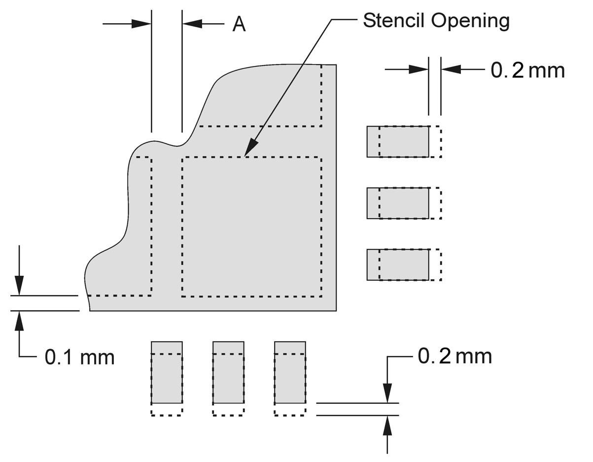
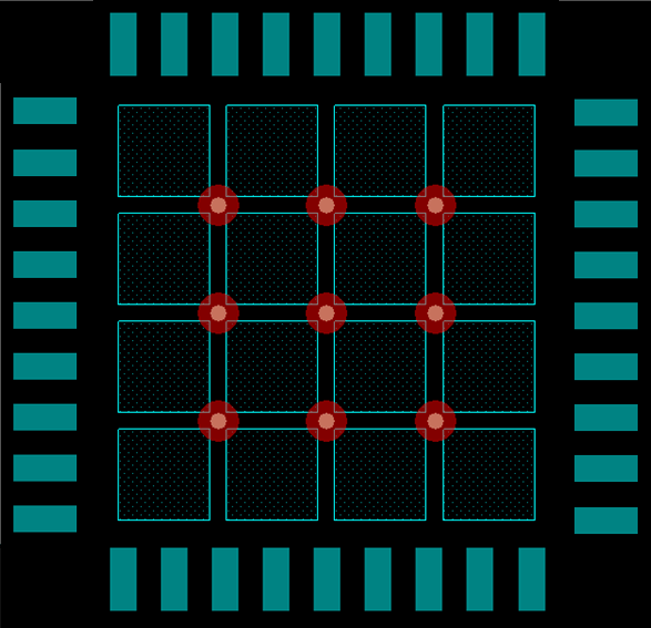
Stencil parameters such as aperture area ratio and the fabrication process have a significant impact on paste deposition. Inspection of the stencil prior to placement of the WQFN package is highly recommended to improve board assembly yields. If the via and aperture openings are not carefully monitored, the solder may flow unevenly through the DAP. Stencil parameters for aperture opening and via locations are shown in Figure 19. A layout example for the DS42MB100 is shown in Figure 20, where 16 stencil openings are used for the DAP alongside nine vias to GND.
 Figure 19. No Pullback WQFN, Single Row Reference Diagram
Table 7. No Pullback WQFN Stencil Aperture Summary for DS42MB100
| DEVICE | PIN COUNT | MKT DWG | PCB I/O PAD SIZE (mm) | PCB PITCH (mm) | PCB DAP SIZE (mm) | STENCIL I/O APERTURE (mm) | STENCIL DAP APERTURE (mm) | NUMBER OF DAP APERTURE OPENINGS |
GAP BETWEEN DAP APERTURE (Dim A mm) |
|---|---|---|---|---|---|---|---|---|---|
| DS42MB100 | 36 | SQA36A | 0.25 × 0.6 | 0.5 | 4.6 × 4.6 | 0.25 × 0.7 | 1.0 × 1.0 | 16 | 0.2 |
 Figure 20. 36-Pin WQFN Stencil Example of Via and Opening Placement