SNLS244H September 2006 – January 2016 DS42MB100
PRODUCTION DATA.
- 1 Features
- 2 Applications
- 3 Description
- 4 Revision History
- 5 Pin Configuration and Functions
- 6 Specifications
- 7 Parameter Measurement Information
- 8 Detailed Description
- 9 Application and Implementation
- 10Power Supply Recommendations
- 11Layout
- 12Device and Documentation Support
- 13Mechanical, Packaging, and Orderable Information
Package Options
Refer to the PDF data sheet for device specific package drawings
Mechanical Data (Package|Pins)
- NJK|36
Thermal pad, mechanical data (Package|Pins)
Orderable Information
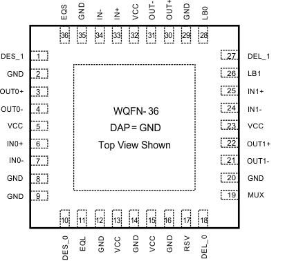
5 Pin Configuration and Functions
NJK Package
36-Pin WQFN
Top View

Pin Functions
| PIN | I/O | DESCRIPTION | |
|---|---|---|---|
| NAME | NO. | ||
| LINE SIDE HIGH SPEED DIFFERENTIAL I/Os | |||
| IN+ IN− |
33 34 |
I | Inverting and non-inverting differential inputs at the line side. IN+ and IN− have an internal 50 Ω connected to an internal reference voltage. See Figure 8. |
| OUT+ OUT− |
30 31 |
O | Inverting and non-inverting differential outputs at the line side. OUT+ and OUT− have an internal 50 Ω connected to VCC. |
| SWITCH SIDE HIGH SPEED DIFFERENTIAL I/Os | |||
| IN0+ IN0− |
6 7 |
I | Inverting and non-inverting differential inputs to the MUX at the switch side. IN0+ and IN0− have an internal 50 Ω connected to an internal reference voltage. See Figure 8. |
| IN1+ IN1− |
25 24 |
I | Inverting and non-inverting differential inputs to the MUX at the switch side. IN1+ and IN1− have an internal 50 Ω connected to an internal reference voltage. See Figure 8. |
| OUT0+ OUT0− |
3 4 |
O | Inverting and non-inverting differential outputs at the switch side. OUT0+ and OUT0− have an internal 50 Ω connected to VCC. |
| OUT1+ OUT1− |
22 21 |
O | Inverting and non-inverting differential outputs at the switch side. OUT1+ and OUT1− have an internal 50 Ω connected to VCC. |
| CONTROL (3.3-V LVCMOS) | |||
| DEL_0 DEL_1 |
18 27 |
I | DEL_0 and DEL_1 select the output pre-emphasis of the line side drivers (OUT±). DEL_0 and DEL_1 are internally pulled high. |
| DES_0 DES_1 |
10 1 |
I | DES_0 and DES_1 select the output pre-emphasis of the switch side drivers (OUT0±, OUT1±). DES_0 and DES_1 are internally pulled high. |
| EQL | 11 | I | A logic low enables the input equalizer on the line side. EQL is internally pulled high. Default is with EQ disabled. |
| EQS | 36 | I | A logic low enables the input equalizer on the switch side. EQS is internally pulled high. Default is with EQ disabled. |
| LB0 | 28 | I | A logic low at LB0 enables the internal loopback path from IN0± to OUT0±. LB0 is internally pulled high. |
| LB1 | 26 | I | A logic low at LB1 enables the internal loopback path from IN1± to OUT1±. LB1 is internally pulled high. |
| MUX | 19 | I | A logic low at MUX selects IN1±. MUX is internally pulled high. Default state for MUX is IN0±. |
| RSV | 17 | I | Reserve pin to support factory testing. This pin can be left open, or tied to GND, or tied to GND through an external pull-down resistor. |
| POWER | |||
| GND | 2, 8, 9, 12, 14, 16, 20, 29, 35 | P | Ground reference. Each ground pin should be connected to the ground plane through a low inductance path, typically with a via located as close as possible to the landing pad of the GND pin. |
| GND | DAP | P | DAP is the metal contact at the bottom side, located at the center of the WQFN package. It should be connected to the GND plane with at least 16 via to lower the ground impedance and improve the thermal performance of the package. |
| VCC | 5, 13, 15, 23, 32 | P | VCC = 3.3 V ± 5%. Each VCC pin should be connected to the VCC plane through a low inductance path, typically with a via located as close as possible to the landing pad of the VCC pin. It is recommended to have a 0.01 μF or 0.1 μF, X7R, size-0402 bypass capacitor from each VCC pin to ground plane. |