SNLS407D April 2012 – October 2014 DS90UB925Q-Q1
PRODUCTION DATA.
- 1 Features
- 2 Applications
- 3 Description
- 4 Revision History
- 5 Pin Configuration and Functions
- 6 Specifications
-
7 Detailed Description
- 7.1 Overview
- 7.2 Functional Block Diagram
- 7.3
Feature Description
- 7.3.1 High Speed Forward Channel Data Transfer
- 7.3.2 Low Speed Back Channel Data Transfer
- 7.3.3 Backward Compatible Mode
- 7.3.4 Common Mode Filter Pin (CMF)
- 7.3.5 Video Control Signal Filter
- 7.3.6 EMI Reduction Features
- 7.3.7 LVCMOS VDDIO Option
- 7.3.8 Power Down (PDB)
- 7.3.9 Remote Auto Power Down Mode
- 7.3.10 Input PCLK Loss Detect
- 7.3.11 Serial Link Fault Detect
- 7.3.12 Pixel Clock Edge Select (RFB)
- 7.3.13 Low Frequency Optimization (LFMODE)
- 7.3.14 Interrupt Pin — Functional Description And Usage (INTB)
- 7.3.15 Internal Pattern Generation
- 7.3.16 GPIO[3:0] and GPO_REG[8:4]
- 7.3.17 I2S Transmitting
- 7.3.18 Built In Self Test (BIST)
- 7.4 Device Functional Modes
- 7.5 Programming
- 7.6 Register Maps
- 8 Application and Implementation
- 9 Power Supply Recommendations
- 10Layout
- 11Device and Documentation Support
- 12Mechanical, Packaging, and Orderable Information
Package Options
Mechanical Data (Package|Pins)
- RHS|48
Thermal pad, mechanical data (Package|Pins)
- RHS|48
Orderable Information
8 Application and Implementation
NOTE
Information in the following applications sections is not part of the TI component specification, and TI does not warrant its accuracy or completeness. TI’s customers are responsible for determining suitability of components for their purposes. Customers should validate and test their design implementation to confirm system functionality.
8.1 Application Information
The DS90UB925Q-Q1, in conjunction with the DS90UB926Q-Q1, is intended for interface between a host (graphics processor) and a Display. It supports a 24-bit color depth (RGB888) and high definition (720p) digital video format. It can receive a three 8-bit RGB stream with a pixel rate up to 85 MHz together with three control bits (VS, HS and DE) and three I2S-bus audio stream with an audio sampling rate up to 192 kHz.
8.2 Typical Application
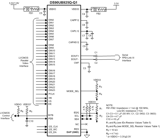 Figure 23. Typical Connection Diagram
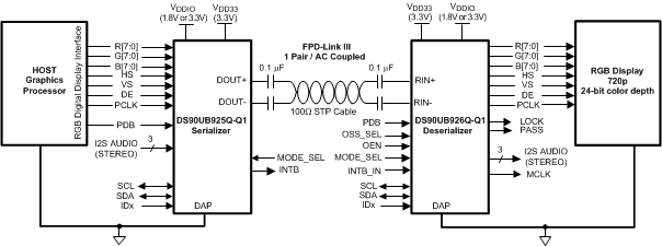 Figure 24. Typical Display System Diagram
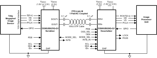 Figure 25. Typical Camera Applications Diagram
8.2.1 Design Requirements
For the typical design application, use the following as input parameters.
Table 7. Design Parameters
| DESIGN PARAMETER | EXAMPLE VALUE |
|---|---|
| VDDIO | 1.8 V or 3.3 V |
| VDD33 | 3.3 V |
| AC Coupling Capacitor for DOUT± | 100 nF |
| PCLK Frequency | 85 MHz |
8.2.2 Detailed Design Procedure
Figure 23 shows a typical application of the DS90UB925Q-Q1 serializer for an 85 MHz 24-bit Color Display Application. The camera application has the same recommended connections. The CML outputs must have an external 0.1 μF AC coupling capacitor on the high speed serial lines. The serializer has an internal termination. Bypass capacitors are placed near the power supply pins. At a minimum, six (6) 4.7μF capacitors and two (2) additional 1μF capacitors should be used for local device bypassing. Ferrite beads are placed on the two (2) VDDs (VDD33 and VDDIO) for effective noise suppression. The interface to the graphics source is with 3.3V LVCMOS levels, thus the VDDIO pin is connected to the 3.3 V rail. A RC delay is placed on the PDB signal to delay the enabling of the device until power is stable.
8.2.3 Application Curves
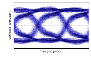 Figure 26. Serializer Eye Diagram with 78 MHz TX Pixel Clock
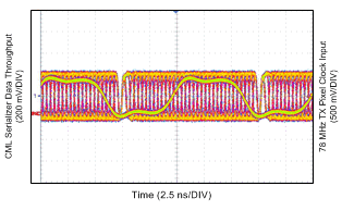 Figure 27. Serializer CML Output with 78 MHz TX Pixel Clock