SNOS521E January 2001 – January 2018 DS92LV040A
PRODUCTION DATA.
- 1 Features
- 2 Applications
- 3 Description
- 4 Revision History
- 5 Pin Configuration and Functions
- 6 Specifications
- 7 Parameter Measurement Information
- 8 Detailed Description
- 9 Application and Implementation
- 10Power Supply Recommendations
- 11Layout
- 12Device and Documentation Support
- 13Mechanical, Packaging, and Orderable Information
Package Options
Mechanical Data (Package|Pins)
- NJN|44
Thermal pad, mechanical data (Package|Pins)
Orderable Information
11.1.6 Decoupling
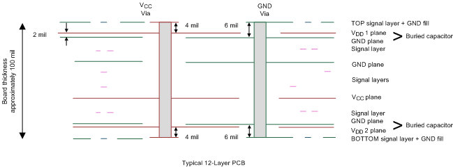
Each power or ground lead of a high-speed device should be connected to the PCB through a low inductance path. For best results, one or more vias are used to connect a power or ground pin to the nearby plane. Ideally, via placement is immediately adjacent to the pin to avoid adding trace inductance. Placing a power plane closer to the top of the board reduces the effective via length and its associated inductance.
 Figure 17. Low Inductance, High-Capacitance Power Connection
Bypass capacitors should be placed close to VDD pins. They can be placed conveniently near the corners or underneath the package to minimize the loop area. This extends the useful frequency range of the added capacitance. Small-physical-size capacitors, such as 0402, 0201, or X7R surface-mount capacitors should be used to minimize body inductance of capacitors. Each bypass capacitor is connected to the power and ground plane through vias tangent to the pads of the capacitor as shown in Figure 18(a).
An X7R surface-mount capacitor of size 0402 has about 0.5 nH of body inductance. At frequencies above 30 MHz or so, X7R capacitors behave as low-impedance inductors. To extend the operating frequency range to a few hundred MHz, an array of different capacitor values like 100 pF, 1 nF, 0.03 μF, and 0.1 μF are commonly used in parallel. The most effective bypass capacitor can be built using sandwiched layers of power and ground at a separation of 2 to 3 mils. With a 2-mil FR4 dielectric, there is approximately 500 pF per square inch of PCB. Many high-speed devices provide a low-inductance GND connection on the backside of the package. This center pad must be connected to a ground plane through an array of vias. The via array reduces the effective inductance to ground and enhances the thermal performance of the small Surface Mount Technology (SMT) package. Placing vias around the perimeter of the pad connection ensures proper heat spreading and the lowest possible die temperature. Placing high-performance devices on opposing sides of the PCB using two GND planes creates multiple paths for heat transfer. Often thermal PCB issues are the result of one device adding heat to another, resulting in a very high local temperature. Multiple paths for heat transfer minimize this possibility. In many cases the GND pad makes the optimal decoupling layout impossible to achieve due to insufficient pad-to-pad spacing as shown in Figure 18(b). When this occurs, placing the decoupling capacitor on the backside of the board keeps the extra inductance to a minimum. It is important to place the VDD via as close to the device pin as possible while still allowing for sufficient solder mask coverage. If the via is left open, solder may flow from the pad and into the via barrel. This results in a poor solder connection.
(a)

(b)
