SBOS772C August   2017  – May 2019 INA1650-Q1 , INA1651-Q1

PRODUCTION DATA.  

  1. Features
  2. Applications
    1.     Simplified Internal Schematic
  3. Description
    1.     CMRR Histogram (5746 Channels)
  4. Revision History
  5. Pin Configuration and Functions
    1.     Pin Functions: INA1650-Q1
    2.     Pin Functions: INA1651-Q1
  6. Specifications
    1. 6.1 Absolute Maximum Ratings
    2. 6.2 ESD Ratings
    3. 6.3 Recommended Operating Conditions
    4. 6.4 Thermal Information
    5. 6.5 Electrical Characteristics:
    6. 6.6 Typical Characteristics
  7. Detailed Description
    1. 7.1 Overview
    2. 7.2 Functional Block Diagram
    3. 7.3 Feature Description
      1. 7.3.1 Audio Signal Path
      2. 7.3.2 Supply Divider
      3. 7.3.3 EMI Rejection
      4. 7.3.4 Electrical Overstress
      5. 7.3.5 Thermal Shutdown
    4. 7.4 Device Functional Modes
      1. 7.4.1 Single-Supply Operation
  8. Application and Implementation
    1. 8.1 Application Information
      1. 8.1.1 Input Common-Mode Range
      2. 8.1.2 Common-Mode Input Impedance
      3. 8.1.3 Start-Up Time in Single-Supply Applications
      4. 8.1.4 Input AC Coupling
      5. 8.1.5 Supply Divider Capacitive Loading
    2. 8.2 Typical Applications
      1. 8.2.1 Line Receiver for Differential Audio Signals in a Split-Supply System
        1. 8.2.1.1 Design Requirements
        2. 8.2.1.2 Detailed Design Procedure
        3. 8.2.1.3 Application Curves
      2. 8.2.2 Two-Channel Microphone Input for Automotive Infotainment Systems
      3. 8.2.3 TRS Audio Interface in Single-Supply Applications
  9. Power Supply Recommendations
  10. 10Layout
    1. 10.1 Layout Guidelines
    2. 10.2 Layout Example
  11. 11Device and Documentation Support
    1. 11.1 Device Support
      1. 11.1.1 Development Support
        1. 11.1.1.1 TINA-TI (Free Software Download)
        2. 11.1.1.2 TI Precision Designs
    2. 11.2 Documentation Support
      1. 11.2.1 Related Documentation
    3. 11.3 Receiving Notification of Documentation Updates
    4. 11.4 Community Resources
    5. 11.5 Trademarks
    6. 11.6 Electrostatic Discharge Caution
    7. 11.7 Glossary
  12. 12Mechanical, Packaging, and Orderable Information

Package Options

Mechanical Data (Package|Pins)
Thermal pad, mechanical data (Package|Pins)
Orderable Information

Supply Divider Capacitive Loading

The VMID(OUT) pin of the INA165x-Q1 is stable with capacitive loads up to 150 pF. An isolation resistor (RISO in Figure 51), must be used if capacitive loads larger than 150 pF are connected to the VMID(OUT) pin. Figure 51 shows the recommended configuration of an isolation resistor in series with the capacitive load. The REF pins of the INA165x-Q1 must connect directly to the VMID(OUT) pin before the isolation resistor. Any resistance placed between the VMID(OUT) pin and the reference pins degrades the CMRR of the device. Figure 52 shows the recommended value for the isolation resistor for increasing capacitive loads.
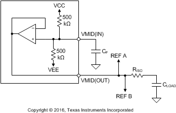
INA1650-Q1 INA1651-Q1 AI_D004.gifFigure 51. Place an Isolation Resistor Between the VMID(OUT) Pin and Large Capacitive Loads
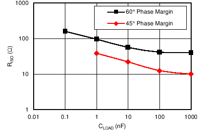
INA1650-Q1 INA1651-Q1 C042_SBOS618.pngFigure 52. Recommended Isolation Resistor Value vs Capacitive Load