SBOS318B April 2019 – July 2021 INA186
PRODUCTION DATA
- 1 Features
- 2 Applications
- 3 Description
- 4 Revision History
- 5 Pin Configuration and Functions
- 6 Specifications
- 7 Detailed Description
- 8 Application and Implementation
- 9 Power Supply Recommendations
- 10Layout
- 11Device and Documentation Support
- 12Mechanical, Packaging, and Orderable Information
Package Options
Refer to the PDF data sheet for device specific package drawings
Mechanical Data (Package|Pins)
- DDF|8
- YFD|6
- DCK|6
Thermal pad, mechanical data (Package|Pins)
- DCK|6
Orderable Information
8.1.2 RSENSE and Device Gain Selection
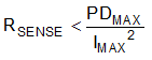
The accuracy of any current-sense amplifier is maximized by choosing the current-sense resistor to be as large as possible. A large sense resistor maximizes the differential input signal for a given amount of current flow and reduces the error contribution of the offset voltage. However, there are practical limits as to how large the current-sense resistor can be in a given application because of the resistor size and maximum allowable power dissipation. Equation 2 gives the maximum value for the current-sense resistor for a given power dissipation budget:
where:
- PDMAX is the maximum allowable power dissipation in RSENSE.
- IMAX is the maximum current that will flow through RSENSE.
An additional limitation on the size of the current-sense resistor and device gain is due to the power-supply voltage, VS, and device swing-to-rail limitations. In order to make sure that the current-sense signal is properly passed to the output, both positive and negative output swing limitations must be examined. Equation 3 provides the maximum values of RSENSE and GAIN to keep the device from exceeding the positive swing limitation.

where:
- IMAX is the maximum current that will flow through RSENSE.
- GAIN is the gain of the current-sense amplifier.
- VSP is the positive output swing as specified in the data sheet.
- VREF is the externally applied voltage on the REF pin. This voltage is zero for devices without a REF pin.
To avoid positive output swing limitations when selecting the value of RSENSE, there is always a trade-off between the value of the sense resistor and the gain of the device under consideration. If the sense resistor selected for the maximum power dissipation is too large, then it is possible to select a lower-gain device in order to avoid positive swing limitations.
The negative swing limitation places a limit on how small the sense resistor value can be for a given application. Equation 4 provides the limit on the minimum value of the sense resistor.

where:
- IMIN is the minimum current that will flow through RSENSE.
- GAIN is the gain of the current-sense amplifier.
- VSN is the negative output swing of the device (see Section 7.3.7).
- VREF is the externally applied voltage on the REF pin. This voltage is zero for devices without a REF pin.
In addition to adjusting RSENSE and the device gain, the voltage applied to the REF pin can be slightly increased above GND to avoid negative swing limitations.