SBOS562G August   2011  – June 2020 INA826

PRODUCTION DATA.  

  1. Features
  2. Applications
  3. Description
    1.     Device Images
      1.      General-Purpose Instrumentation Amplifier
  4. Revision History
  5. Device Comparison Table
  6. Pin Configuration and Functions
    1.     Pin Functions
  7. Specifications
    1. 7.1 Absolute Maximum Ratings
    2. 7.2 ESD Ratings
    3. 7.3 Recommended Operating Conditions
    4. 7.4 Thermal Information
    5. 7.5 Electrical Characteristics
    6. 7.6 Typical Characteristics
  8. Detailed Description
    1. 8.1 Overview
    2. 8.2 Functional Block Diagram
    3. 8.3 Feature Description
      1. 8.3.1  Inside the INA826
      2. 8.3.2  Setting the Gain
        1. 8.3.2.1 Gain Drift
      3. 8.3.3  Offset Trimming
      4. 8.3.4  Input Common-Mode Range
      5. 8.3.5  Input Protection
      6. 8.3.6  Input Bias Current Return Path
      7. 8.3.7  Reference Terminal
      8. 8.3.8  Dynamic Performance
      9. 8.3.9  Operating Voltage
        1. 8.3.9.1 Low-Voltage Operation
      10. 8.3.10 Error Sources
    4. 8.4 Device Functional Modes
  9. Application and Implementation
    1. 9.1 Application Information
    2. 9.2 Typical Application
      1. 9.2.1 Design Requirements
      2. 9.2.2 Detailed Design Procedure
      3. 9.2.3 Application Curves
    3. 9.3 System Examples
      1. 9.3.1 Circuit Breaker
      2. 9.3.2 Programmable Logic Controller (PLC) Input
      3. 9.3.3 Using TINA-TI SPICE-Based Analog Simulation Program With the INA826
  10. 10Power Supply Recommendations
  11. 11Layout
    1. 11.1 Layout Guidelines
      1. 11.1.1 CMRR vs Frequency
    2. 11.2 Layout Example
  12. 12Device and Documentation Support
    1. 12.1 Documentation Support
      1. 12.1.1 Related Documentation
    2. 12.2 Receiving Notification of Documentation Updates
    3. 12.3 Support Resources
    4. 12.4 Trademarks
    5. 12.5 Electrostatic Discharge Caution
    6. 12.6 Glossary
  13. 13Mechanical, Packaging, and Orderable Information

Package Options

Mechanical Data (Package|Pins)
Thermal pad, mechanical data (Package|Pins)
Orderable Information

Offset Trimming

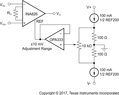
Most applications require no external offset adjustment; however, if necessary, adjustments can be made by applying a voltage to the REF terminal. Figure 59 shows an optional circuit for trimming the output offset voltage. The voltage applied to the REF terminal is summed at the output. The op amp buffer provides low impedance at the REF terminal to preserve good common-mode rejection.
INA826 ai_opt_trim_vo_bos562.gifFigure 59. Optional Trimming of the Output Offset Voltage