SBOS945B November 2020 – April 2021 INA849
PRODUCTION DATA
- 1 Features
- 2 Applications
- 3 Description
- 4 Revision History
- 5 Device Comparison Table
- 6 Pin Configuration and Functions
- 7 Specifications
- 8 Detailed Description
- 9 Application and Implementation
- 10Power Supply Recommendations
- 11Layout
- 12Device and Documentation Support
- 13Mechanical, Packaging, and Orderable Information
Package Options
Mechanical Data (Package|Pins)
Thermal pad, mechanical data (Package|Pins)
Orderable Information
8.3.1 Adjustable Gain Setting
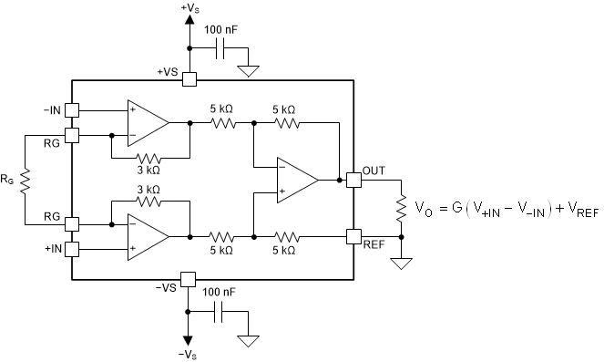
Figure 8-1 shows that the gain of the INA849 is set by a single external resistor (RG) connected between the RG pins (pins 2 and 3).
 Figure 8-1 Simplified Diagram of the INA849 with
Output Equation
Figure 8-1 Simplified Diagram of the INA849 with
Output EquationThe value of RG is selected according to the following equation:

Table 8-1 lists several commonly used gains and resistor values. The 6-kΩ term in Equation 1 is a result of the sum of the two internal 3-kΩ feedback resistors. These on-chip resistors are laser-trimmed to accurate, absolute values. The accuracy and temperature coefficients of these resistors are included in the gain accuracy and drift specifications of the INA849.
| DESIRED GAIN (V/V) | STANDARD 1% RG (Ω) | CALCULATED GAIN (V/V) | CALCULATED GAIN ERROR (%) |
|---|---|---|---|
| 1 | Not connected | N/A | N/A |
| 2 | 6.04 k | 1.9933 | 0.33 |
| 5 | 1.50 k | 5 | 0 |
| 10 | 665 | 10.022 | –0.23 |
| 20 | 316 | 19.987 | 0.06 |
| 50 | 121 | 50.586 | –1.17 |
| 100 | 60.4 | 100.337 | –0.34 |
| 200 | 30.1 | 200.335 | –0.17 |
| 500 | 12.1 | 496.867 | 0.63 |
| 1000 | 6.04 | 994.377 | 0.56 |
The 5-kΩ feedback resistors in the output stage are ratiometrically matched to achieve unity-gain stability. These resistors may shift up to 15% depending on production.
As shown in Figure 8-1 and explained in more detail in Figure 11-1, make sure to connect low-ESR, 0.1-µF, ceramic bypass capacitors between each supply pin and ground, placed as close to the device as possible.