SBOS938C October 2018 – June 2020 INA901-SP
PRODUCTION DATA.
- 1 Features
- 2 Applications
- 3 Description
- 4 Revision History
- 5 Pin Configuration and Functions
- 6 Specifications
- 7 Detailed Description
- 8 Application and Implementation
- 9 Power Supply Recommendations
- 10Layout
- 11Device and Documentation Support
- 12Mechanical, Packaging, and Orderable Information
Package Options
Mechanical Data (Package|Pins)
- HKX|8
Thermal pad, mechanical data (Package|Pins)
Orderable Information
3 Description
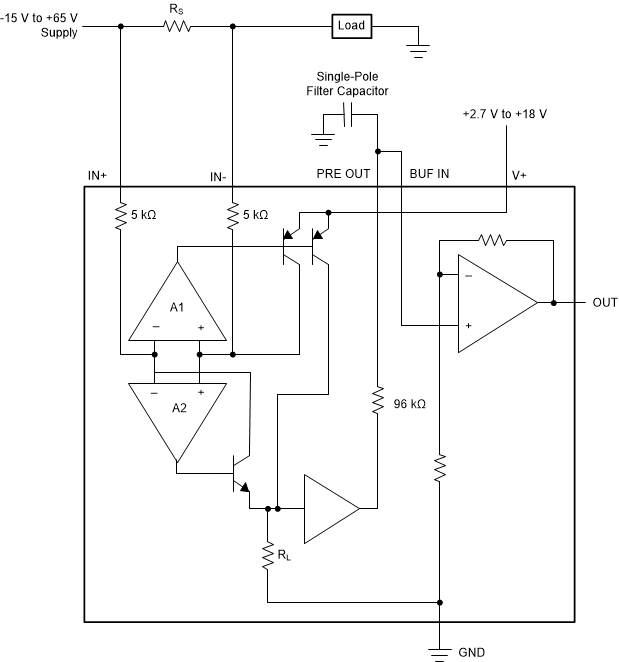
The INA901-SP is a voltage-output, current-sense amplifier that can sense drops across shunt resistors at common-mode voltages from –15 V to 65 V, independent of the supply voltage. The INA901-SP operates from a single 2.7-V to 16-V supply, drawing 700 μA (typical) of supply current.
The gain of the INA901-SP is 20 V/V. The 130-kHz bandwidth simplifies use in current-control loops. The pinouts readily enable filtering.
The device is specified over the extended operating temperature range of –55 °C to 125 °C and is offered in an 8-pin CFP package.
Device Information(1)
| PART NUMBER | GRADE | PACKAGE |
|---|---|---|
| 5962L1821001VXC | QMLV RHA
[50 krad(Si)] |
8-lead CFP [HKX]
6.48 × 6.48 mm Weight: 0.39 g(3) |
| 5962-1821001VXC | QMLV | |
| INA901HKX/EM | Engineering Samples(2) | |
| INA901EVM-CVAL | Ceramic Evaluation Board | — |
- For all available packages, see the orderable addendum at the end of the data sheet.
- These units are intended for engineering evaluation only. They are processed to a noncompliant flow. These units are not suitable for qualification, production, radiation testing or flight use. Parts are not warranted for performance over the full MIL specified temperature range of –55 °C to 125 °C or operating life.
- Weight is accurate to ±10%.
Simplified Schematic
