SLOS581J may 2008 – august 2023 ISO3080 , ISO3082 , ISO3086 , ISO3088
PRODUCTION DATA
- 1
- 1 Features
- 2 Applications
- 3 Description
- 4 Revision History
- 5 Pin Configuration and Functions
-
6 Specifications
- 6.1 Absolute Maximum Ratings
- 6.2 ESD Ratings
- 6.3 Recommended Operating Conditions
- 6.4 Thermal Information
- 6.5 Insulation Specifications
- 6.6 Safety-Related Certifications
- 6.7 Safety Limiting Values
- 6.8 Electrical Characteristics: Driver
- 6.9 Electrical Characteristics: Receiver
- 6.10 Supply Current
- 6.11 Switching Characteristics: Driver
- 6.12 Switching Characteristics: Receiver
- 6.13 Insulation Characteristics Curves
- 6.14 Typical Characteristics
- 7 Parameter Measurement Information
- 8 Detailed Description
- 9 Application and Implementation
- 10Power Supply Recommendations
- 11Layout
- 12Device and Documentation Support
- 13Mechanical, Packaging, and Orderable Information
Package Options
Refer to the PDF data sheet for device specific package drawings
Mechanical Data (Package|Pins)
- DW|16
Thermal pad, mechanical data (Package|Pins)
Orderable Information
5 Pin Configuration and Functions
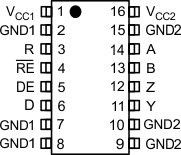
 Figure 5-1 ISO3080 and ISO3086 DW Package16-Pin SOICTop View
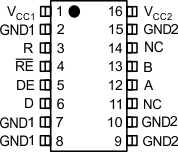
 Figure 5-2 ISO3082 and ISO3088 DW Package16-Pin SOICTop View
Table 5-1 Pin Functions
| PIN | I/O | DESCRIPTION | ||
|---|---|---|---|---|
| NAME | ISO3080, ISO3086 |
ISO3082, ISO3088 |
||
| A | 14 | — | I | Receiver noninverting input on the bus-side |
| — | 12 | I/O | Transceiver noninverting Input or output (I/O) on the bus-side | |
| B | 13 | — | I | Receiver inverting Input on the bus-side |
| — | 13 | I/O | Transceiver inverting input or output (I/O) on the bus-side | |
| D | 6 | 6 | I | Driver input |
| DE | 5 | 5 | I | Enables (when high) or disables (when low or open) driver output of ISO308x |
| GND1 | 2 | 2 | — | Ground connection for VCC1 |
| 7 | 7 | |||
| 8 | 8 | |||
| GND2 | 9 | 9 | — | Ground connection for VCC2 |
| 10 | 10 | |||
| 15 | 15 | |||
| NC | — | 11 | — | No connect |
| 14 | ||||
| R | 3 | 3 | O | Receiver output |
| RE | 4 | 4 | I | Disables (when high or open) or enables (when low) receiver output of ISO308x |
| VCC1 | 1 | 1 | — | Power supply, VCC1 |
| VCC2 | 16 | 16 | — | Power supply, VCC2 |
| Y | 11 | — | O | Driver noninverting output |
| Z | 12 | — | O | Driver inverting output |