SLLSE83F April 2013 – January 2015 ISO7131CC , ISO7140CC , ISO7140FCC , ISO7141CC , ISO7141FCC
PRODUCTION DATA.
- 1 Features
- 2 Applications
- 3 Description
- 4 Revision History
- 5 Pin Configuration and Functions
-
6 Specifications
- 6.1 Absolute Maximum Ratings
- 6.2 ESD Ratings
- 6.3 Recommended Operating Conditions
- 6.4 Thermal Information
- 6.5 Power Dissipation Ratings
- 6.6 Electrical Characteristics: VCC1 and VCC2 at 5 V ±10%
- 6.7 Electrical Characteristics: VCC1 and VCC2 at 3.3 V ±10%
- 6.8 Electrical Characteristics: VCC1 and VCC2 at 2.7 V
- 6.9 Switching Characteristics: VCC1 and VCC2 at 5 V ±10%
- 6.10 Switching Characteristics: VCC1 and VCC2 at 3.3 V ±10%
- 6.11 Switching Characteristics: VCC1 and VCC2 at 2.7 V
- 6.12 Supply Current: VCC1 and VCC2 at 5 V ±10%
- 6.13 Supply Current: VCC1 and VCC2 at 3.3 V ±10%
- 6.14 Supply Current: VCC1 and VCC2 at 2.7 V
- 6.15 Typical Characteristics
- 7 Parameter Measurement Information
- 8 Detailed Description
- 9 Application and Implementation
- 10Power Supply Recommendations
- 11Layout
- 12Device and Documentation Support
- 13Mechanical, Packaging, and Orderable Information
Package Options
Mechanical Data (Package|Pins)
- DBQ|16
Thermal pad, mechanical data (Package|Pins)
Orderable Information
1 Features
- Maximum Signaling Rate: 50 Mbps (With 5-V Supplies)
- Robust Design With Integrated Noise Filter
- Default Output Low Option (Suffix F)
- Low Power Consumption, Typical ICC per Channel (With 3.3-V Supplies):
- Low Propagation Delay: 23-ns Typical
(3.3-V Supplies) - Wide Temperature Range: –40°C to 125°C
- 50-kV/µs Transient Immunity, Typical
- Long Life With SiO2 Isolation Barrier
- Operates from 2.7-V, 3.3-V, and 5-V Supply and Logic Levels
- Small QSOP-16 Package
- Safety and Regulatory Approvals
2 Applications
3 Description
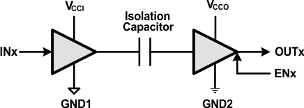
ISO7131, ISO7140, and ISO7141 devices provide galvanic isolation up to 2500 VRMS for 1 minute per UL and 4242 VPK per VDE. ISO7131 has three channels with two forward and one reverse-direction channels. ISO7140 and ISO7141 are quad-channel isolators; ISO7140 has four forward channels, ISO7141 has three forward and one reverse-direction channels. These devices are capable of 50-Mbps maximum data rate with 5-V supplies and 40-Mbps maximum data rate with 3.3-V or 2.7-V supplies, with integrated filters on the inputs for noise-prone applications. The suffix F indicates that default output state is low; otherwise, the default output state is high (see Table 3).
Each isolation channel has a logic input and output buffer separated by a silicon dioxide (SiO2) insulation barrier. Used with isolated power supplies, these devices prevent noise currents on a data bus or other circuits from entering the local ground and interfering with or damaging sensitive circuitry. The devices have TTL input thresholds and can operate from 2.7-V, 3.3-V, and 5-V supplies. All inputs are 5-V tolerant when supplied from a 2.7-V or 3.3-V supply.
Device Information(1)
| PART NUMBER | PACKAGE | BODY SIZE (NOM) |
|---|---|---|
| ISO7131CC | SSOP (16) | 4.90 mm × 3.90 mm |
| ISO7140CC | ||
| ISO7140FCC | ||
| ISO7141CC | ||
| ISO7141FCC |
- For all available packages, see the orderable addendum at the end of the datasheet.