SLLSE83F April 2013 – January 2015 ISO7131CC , ISO7140CC , ISO7140FCC , ISO7141CC , ISO7141FCC
PRODUCTION DATA.
- 1 Features
- 2 Applications
- 3 Description
- 4 Revision History
- 5 Pin Configuration and Functions
-
6 Specifications
- 6.1 Absolute Maximum Ratings
- 6.2 ESD Ratings
- 6.3 Recommended Operating Conditions
- 6.4 Thermal Information
- 6.5 Power Dissipation Ratings
- 6.6 Electrical Characteristics: VCC1 and VCC2 at 5 V ±10%
- 6.7 Electrical Characteristics: VCC1 and VCC2 at 3.3 V ±10%
- 6.8 Electrical Characteristics: VCC1 and VCC2 at 2.7 V
- 6.9 Switching Characteristics: VCC1 and VCC2 at 5 V ±10%
- 6.10 Switching Characteristics: VCC1 and VCC2 at 3.3 V ±10%
- 6.11 Switching Characteristics: VCC1 and VCC2 at 2.7 V
- 6.12 Supply Current: VCC1 and VCC2 at 5 V ±10%
- 6.13 Supply Current: VCC1 and VCC2 at 3.3 V ±10%
- 6.14 Supply Current: VCC1 and VCC2 at 2.7 V
- 6.15 Typical Characteristics
- 7 Parameter Measurement Information
- 8 Detailed Description
- 9 Application and Implementation
- 10Power Supply Recommendations
- 11Layout
- 12Device and Documentation Support
- 13Mechanical, Packaging, and Orderable Information
Package Options
Mechanical Data (Package|Pins)
- DBQ|16
Thermal pad, mechanical data (Package|Pins)
Orderable Information
5 Pin Configuration and Functions
16-Pin
SSOP Package
Top View
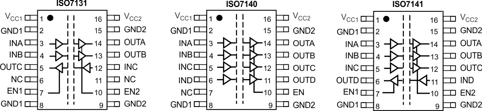
Pin Functions
| PIN | I/O | DESCRIPTION | |||
|---|---|---|---|---|---|
| NAME | ISO7131 | ISO7140 | ISO7141 | ||
| EN | — | 10 | — | I | Output enable. All output pins are enabled when EN is high or disconnected and disabled when EN is low. |
| EN1 | 7 | — | 7 | I | Output enable 1. Output pins on side-1 are enabled when EN1 is high or disconnected and disabled when EN1 is low. |
| EN2 | 10 | — | 10 | I | Output enable 2. Output pins on side-2 are enabled when EN2 is high or disconnected and disabled when EN2 is low. |
| GND1 | 2,8 | 2,8 | 2,8 | — | Ground connection for VCC1 |
| GND2 | 9,15 | 9,15 | 9,15 | — | Ground connection for VCC2 |
| INA | 3 | 3 | 3 | I | Input, channel A |
| INB | 4 | 4 | 4 | I | Input, channel B |
| INC | 12 | 5 | 5 | I | Input, channel C |
| IND | — | 6 | 11 | I | Input, channel D |
| NC | 6,11 | 7 | — | — | No Connect pins are floating with no internal connection |
| OUTA | 14 | 14 | 14 | O | Output, channel A |
| OUTB | 13 | 13 | 13 | O | Output, channel B |
| OUTC | 5 | 12 | 12 | O | Output, channel C |
| OUTD | — | 11 | 6 | O | Output, channel D |
| VCC1 | 1 | 1 | 1 | — | Power supply, VCC1 |
| VCC2 | 16 | 16 | 16 | — | Power supply, VCC2 |