SLLSE83F April 2013 – January 2015 ISO7131CC , ISO7140CC , ISO7140FCC , ISO7141CC , ISO7141FCC
PRODUCTION DATA.
- 1 Features
- 2 Applications
- 3 Description
- 4 Revision History
- 5 Pin Configuration and Functions
-
6 Specifications
- 6.1 Absolute Maximum Ratings
- 6.2 ESD Ratings
- 6.3 Recommended Operating Conditions
- 6.4 Thermal Information
- 6.5 Power Dissipation Ratings
- 6.6 Electrical Characteristics: VCC1 and VCC2 at 5 V ±10%
- 6.7 Electrical Characteristics: VCC1 and VCC2 at 3.3 V ±10%
- 6.8 Electrical Characteristics: VCC1 and VCC2 at 2.7 V
- 6.9 Switching Characteristics: VCC1 and VCC2 at 5 V ±10%
- 6.10 Switching Characteristics: VCC1 and VCC2 at 3.3 V ±10%
- 6.11 Switching Characteristics: VCC1 and VCC2 at 2.7 V
- 6.12 Supply Current: VCC1 and VCC2 at 5 V ±10%
- 6.13 Supply Current: VCC1 and VCC2 at 3.3 V ±10%
- 6.14 Supply Current: VCC1 and VCC2 at 2.7 V
- 6.15 Typical Characteristics
- 7 Parameter Measurement Information
- 8 Detailed Description
- 9 Application and Implementation
- 10Power Supply Recommendations
- 11Layout
- 12Device and Documentation Support
- 13Mechanical, Packaging, and Orderable Information
Package Options
Mechanical Data (Package|Pins)
- DBQ|16
Thermal pad, mechanical data (Package|Pins)
Orderable Information
8 Detailed Description
8.1 Overview
The isolator in Figure 14 is based on a capacitive isolation barrier technique. The I/O channel of the device consists of two internal data channels, a high-frequency channel (HF) with a bandwidth from 100 kbps up to
150 Mbps, and a low-frequency channel (LF) covering the range from 100 kbps down to DC. In principle, a single-ended input signal entering the HF-channel is split into a differential signal through the inverter gate at the input. The following capacitor-resistor networks differentiate the signal into transients, which then are converted into differential pulses by two comparators. The comparator outputs drive a NOR-gate flip-flop whose output feeds an output multiplexer. A decision logic (DCL) at the driving output of the flip-flop measures the durations between signal transients. If the duration between two consecutive transients exceeds a certain time limit, (as in the case of a low-frequency signal), the DCL forces the output-multiplexer to switch from the high- to the low-frequency channel.
Because low-frequency input signals require the internal capacitors to assume prohibitively large values, these signals are pulse-width modulated (PWM) with the carrier frequency of an internal oscillator, thus creating a sufficiently high frequency signal, capable of passing the capacitive barrier. As the input is modulated, a low-pass filter (LPF) is needed to remove the high-frequency carrier from the actual data before passing it on to the output multiplexer.
8.2 Functional Block Diagram
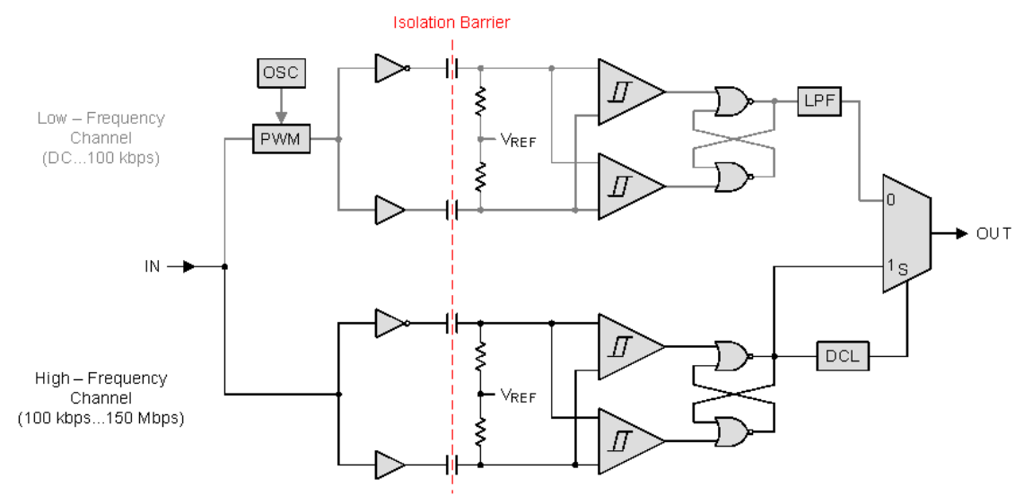 Figure 14. Conceptual Block Diagram of a Digital Capacitive Isolator
8.3 Feature Description
Table 1. Product Features
| PRODUCT | RATED ISOLATION |
INPUT THRESHOLD |
DEFAULT OUTPUT |
MAX DATA RATE and INPUT FILTER |
CHANNEL DIRECTION |
|
|---|---|---|---|---|---|---|
| ISO7131CC | 4242 VPK(1) | 1.5-V TTL (CMOS compatible) |
High | 50 Mbps, with noise filter integrated |
2 forward, 1 reverse |
|
| ISO7140CC | 4 forward, 0 reverse |
|||||
| ISO7140FCC | Low | |||||
| ISO7141CC | High | 3 forward, 1 reverse |
||||
| ISO7141FCC | Low | |||||
8.3.1 Insulation and Safety-Related Specifications
| PARAMETER | TEST CONDITIONS | MIN | TYP | MAX | UNIT | ||
|---|---|---|---|---|---|---|---|
| VIOTM | Maximum transient overvoltage per DIN V VDE V 0884-10 (VDE V 0884-10):2006-12 | 4242 | VPK | ||||
| VIORM | Maximum working voltage per DIN V VDE V 0884-10 (VDE V 0884-10):2006-12 | 566 | VPK | ||||
| VISO | Isolation Voltage per UL 1577 | VTEST = VISO, t = 60 sec (qualification) | 2500 | VRMS | |||
| VTEST = 1.2 * VISO, t = 1 sec (100% production) | 3000 | ||||||
| VPR | Input-to-output test voltage per DIN V VDE V 0884-10 (VDE V 0884-10):2006-12 | After Input/Output safety test subgroup 2/3, VPR = VIORM x 1.2, t = 10 s, Partial discharge < 5 pC |
679 | VPK | |||
| Method a, After environmental tests subgroup 1, VPR = VIORM x 1.6, t = 10 s, Partial discharge < 5 pC |
906 | ||||||
| Method b1, 100% production test, VPR = VIORM x 1.875, t = 1 s, Partial discharge < 5 pC |
1061 | ||||||
| L(I01) | Minimum air gap (clearance) | Shortest terminal to terminal distance through air | 3.7 | mm | |||
| L(I02) | Minimum external tracking (creepage) | Shortest terminal to terminal distance across the package surface | 3.7 | mm | |||
| Minimum internal gap (internal clearance) | Distance through the insulation | 0.014 | mm | ||||
| Pollution degree | 2 | ||||||
| CTI | Tracking resistance (comparative tracking index) | DIN IEC 60112 / VDE 0303 Part 1 | ≥400 | V | |||
| RIO(1) | Isolation Resistance, Input to Output | VIO = 500 V, TA = 25oC | >1012 | Ω | |||
| VIO = 500 V, 100oC ≤ TA ≤ TA max | >1011 | ||||||
| CIO(1) | Barrier capacitance, input to output | VI = 0.4 sin (2πft), f = 1 MHz | 2.3 | pF | |||
| CI(2) | Input capacitance | VI = VCC/2 + 0.4 sin (2πft), f = 1 MHz, VCC = 5 V | 2.8 | pF | |||
NOTE
Creepage and clearance requirements should be applied according to the specific equipment isolation standards of an application. Care should be taken to maintain the creepage and clearance distance of a board design to ensure that the mounting pads of the isolator on the printed-circuit-board (PCB) do not reduce this distance.
Creepage and clearance on a PCB become equal in certain cases. Techniques such as inserting grooves and/or ribs on a PCB are used to help increase these specifications.
Table 2. IEC 60664-1 Ratings Table
| PARAMETER | TEST CONDITIONS | SPECIFICATION |
|---|---|---|
| Basic Isolation Group | Material Group | II |
| Installation classification | Rated mains voltage ≤ 150 VRMS | I–IV |
| Rated mains voltage ≤ 300 VRMS | I–III | |
| Rated mains voltage ≤ 400 VRMS | I–II |
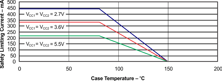
8.3.1.1 Safety Limiting Values
Safety limiting intends to prevent potential damage to the isolation barrier upon failure of input or output circuitry. A failure of the IO can allow low resistance to ground or the supply and, without current limiting, dissipate sufficient power to overheat the die and damage the isolation barrier, potentially leading to secondary system failures.
| PARAMETER | TEST CONDITIONS | MIN | TYP | MAX | UNIT | ||
|---|---|---|---|---|---|---|---|
| IS | Safety input, output, or supply current | DBQ-16 | RθJA = 104.5°C/W, VI = 5.5V, TJ = 150°C, TA = 25°C | 217 | mA | ||
| RθJA = 104.5°C/W, VI = 3.6V, TJ = 150°C, TA = 25°C | 332 | ||||||
| RθJA = 104.5°C/W, VI = 2.7V, TJ = 150°C, TA = 25°C | 443 | ||||||
| TS | Maximum case temperature | 150 | °C | ||||
The safety-limiting constraint is the absolute-maximum junction temperature specified in the Absolute Maximum Ratings table. The power dissipation and junction-to-air thermal impedance of the device installed in the application hardware determines the junction temperature. The assumed junction-to-air thermal resistance in the Thermal Information table is that of a device installed on a high-K test board for leaded surface-mount packages. The power is the recommended maximum input voltage times the current. The junction temperature is then the ambient temperature plus the power times the junction-to-air thermal resistance.
8.3.1.2 Regulatory Information
| VDE | UL | CSA | CQC |
|---|---|---|---|
| Certified according to DIN V VDE V 0884-10 (VDE V 0884-10):2006-12 and DIN EN 61010-1 | Recognized under UL 1577 Component Recognition Program | Approved under CSA Component Acceptance Notice 5A, IEC 60950-1, and IEC 61010-1 | Certified according to GB 4943.1-2011 |
| Basic Insulation Maximum Transient Overvoltage, 4242 VPK Maximum Working Voltage, 566 VPK |
Single protection, 2500 VRMS(1) | Reinforced Insulation per CSA 60950-1-03 and IEC 60950-1 (2nd Ed.), 185 VRMS maximum working voltage Basic Insulation per CSA 60950-1-03 and IEC 60950-1 (2nd Ed.), 370 VRMS maximum working voltage Reinforced Insulation per CSA 61010-1-12 and IEC 61010-1 (3rd Edition), 150 VRMS maximum working voltage Basic Insulation per CSA 61010-1-12 and IEC 61010-1 (3rd Edition), 300 VRMS maximum working voltage |
Basic Insulation, Altitude ≤ 5000m, Tropical Climate, 250 VRMS maximum working voltage |
| Certificate number: 40016131 | File number: E181974 | Master contract number: 220991 | Certificate number: CQC14001109540 |
8.4 Device Functional Modes
Table 3. Function Table(1)
| VCCI | VCCO | INPUT (INx) |
OUTPUT ENABLE (ENx) |
OUTPUT (OUTx) | |
|---|---|---|---|---|---|
| ISO71xxCC | ISO71xxFCC | ||||
| PU | PU | H | H or open | H | H |
| L | H or open | L | L | ||
| X | L | Z | Z | ||
| Open | H or open | H | L | ||
| PD | PU | X | H or open | H | L |
| PD | PU | X | L | Z | Z |
| PU | PD | X | X | Undetermined | Undetermined |
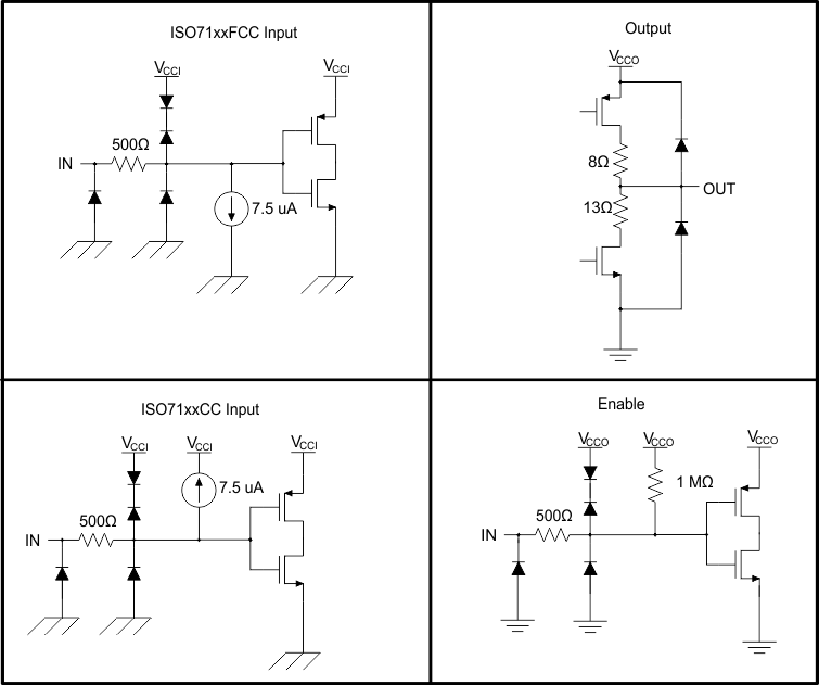 Figure 16. Device I/O Schematics