SLLSE83F April 2013 – January 2015 ISO7131CC , ISO7140CC , ISO7140FCC , ISO7141CC , ISO7141FCC
PRODUCTION DATA.
- 1 Features
- 2 Applications
- 3 Description
- 4 Revision History
- 5 Pin Configuration and Functions
-
6 Specifications
- 6.1 Absolute Maximum Ratings
- 6.2 ESD Ratings
- 6.3 Recommended Operating Conditions
- 6.4 Thermal Information
- 6.5 Power Dissipation Ratings
- 6.6 Electrical Characteristics: VCC1 and VCC2 at 5 V ±10%
- 6.7 Electrical Characteristics: VCC1 and VCC2 at 3.3 V ±10%
- 6.8 Electrical Characteristics: VCC1 and VCC2 at 2.7 V
- 6.9 Switching Characteristics: VCC1 and VCC2 at 5 V ±10%
- 6.10 Switching Characteristics: VCC1 and VCC2 at 3.3 V ±10%
- 6.11 Switching Characteristics: VCC1 and VCC2 at 2.7 V
- 6.12 Supply Current: VCC1 and VCC2 at 5 V ±10%
- 6.13 Supply Current: VCC1 and VCC2 at 3.3 V ±10%
- 6.14 Supply Current: VCC1 and VCC2 at 2.7 V
- 6.15 Typical Characteristics
- 7 Parameter Measurement Information
- 8 Detailed Description
- 9 Application and Implementation
- 10Power Supply Recommendations
- 11Layout
- 12Device and Documentation Support
- 13Mechanical, Packaging, and Orderable Information
Package Options
Mechanical Data (Package|Pins)
- DBQ|16
Thermal pad, mechanical data (Package|Pins)
Orderable Information
9 Application and Implementation
NOTE
Information in the following applications sections is not part of the TI component specification, and TI does not warrant its accuracy or completeness. TI’s customers are responsible for determining suitability of components for their purposes. Customers should validate and test their design implementation to confirm system functionality.
9.1 Application Information
ISO71xx use single-ended TTL-logic switching technology. Its supply voltage range is from 3 V to 5.5 V for both supplies, VCC1 and VCC2. When designing with digital isolators, it is important to note that due to the single-ended design structure, digital isolators do not conform to any specific interface standard and are only intended for isolating single-ended CMOS or TTL digital signal lines. The isolator is typically placed between the data controller (that is, μC or UART), and a data converter or a line transceiver, regardless of the interface type or standard.
9.2 Typical Applications
9.2.1 Isolated Data Acquisition System for Process Control
ISO71xx combined with TI's precision analog-to-digital converter and mixed signal micro-controller can create an advanced isolated data acquisition system as shown in Figure 17.
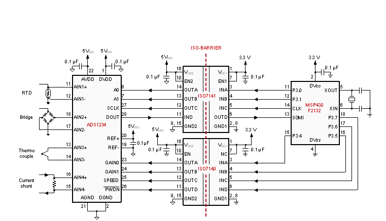 Figure 17. Isolated Data Acquisition System for Process Control
9.2.1.1 Design Requirements
Unlike optocouplers, which need external components to improve performance, provide bias, or limit current, ISO71xx only needs two external bypass capacitors to operate.
9.2.1.2 Detailed Design Procedure
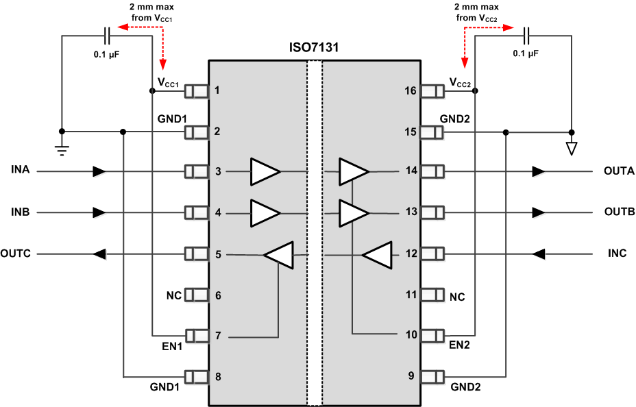 Figure 18. Typical ISO7131 Circuit Hook-up
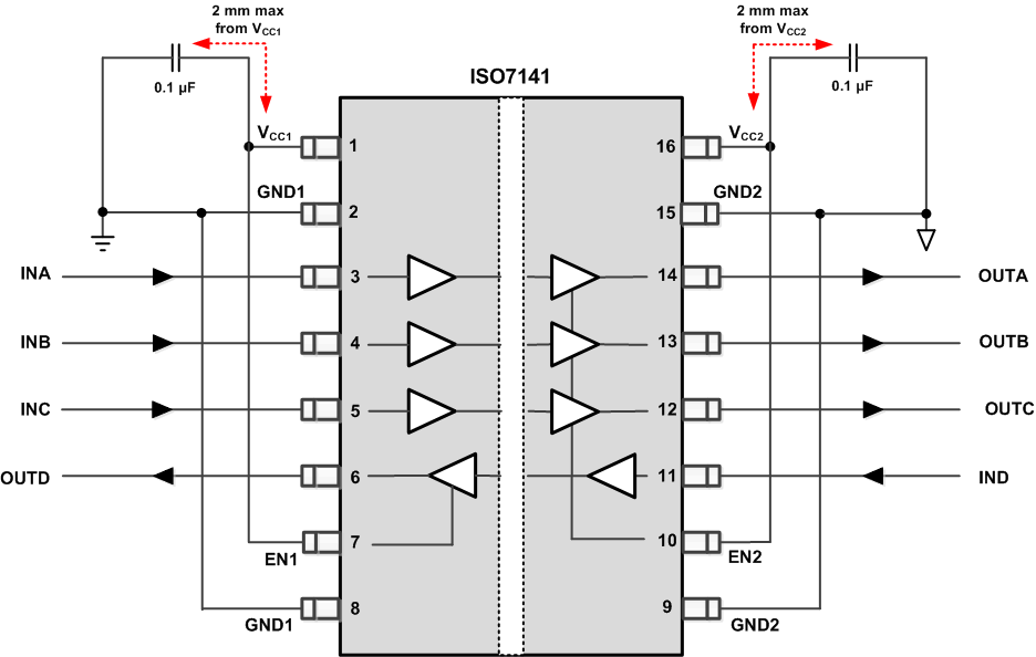 Figure 20. Typical ISO7141 Circuit Hook-up
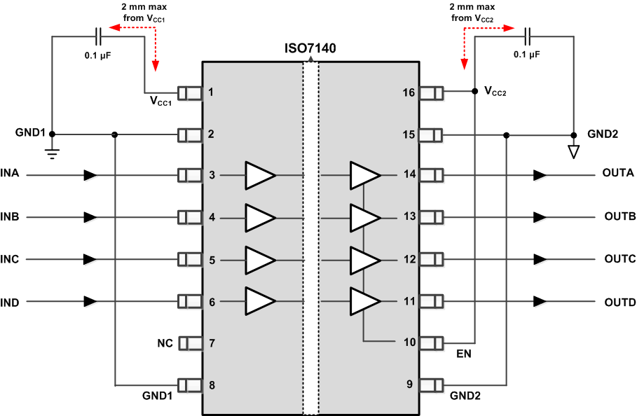 Figure 19. Typical ISO7140 Circuit Hook-up
9.2.2 Isolated RS-485 Interface
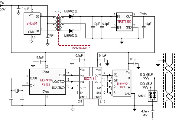 Figure 24. Isolated RS-485 Interface
9.2.2.1 Design Requirements
See previous Design Requirements.
9.2.2.2 Detailed Design Procedure
See previous Detailed Design Procedure.
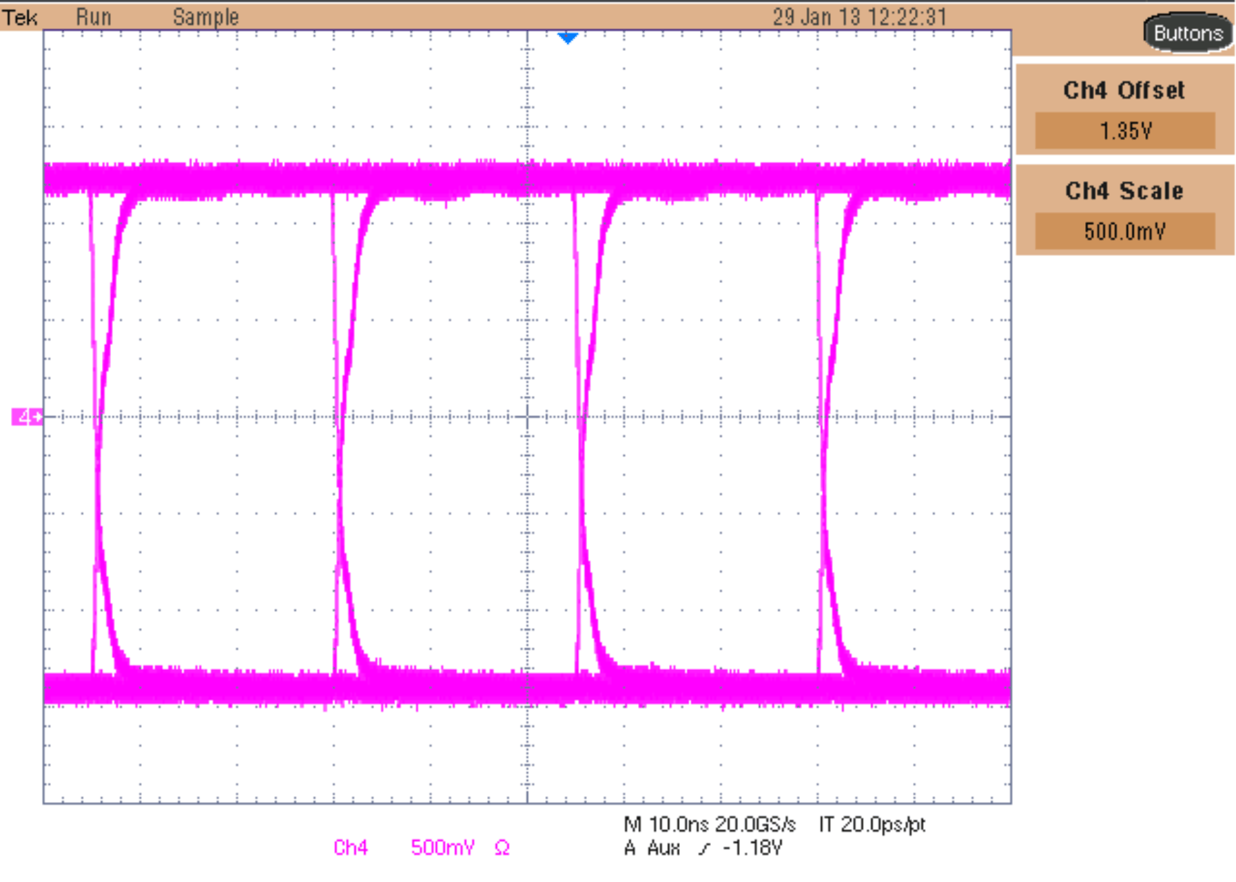
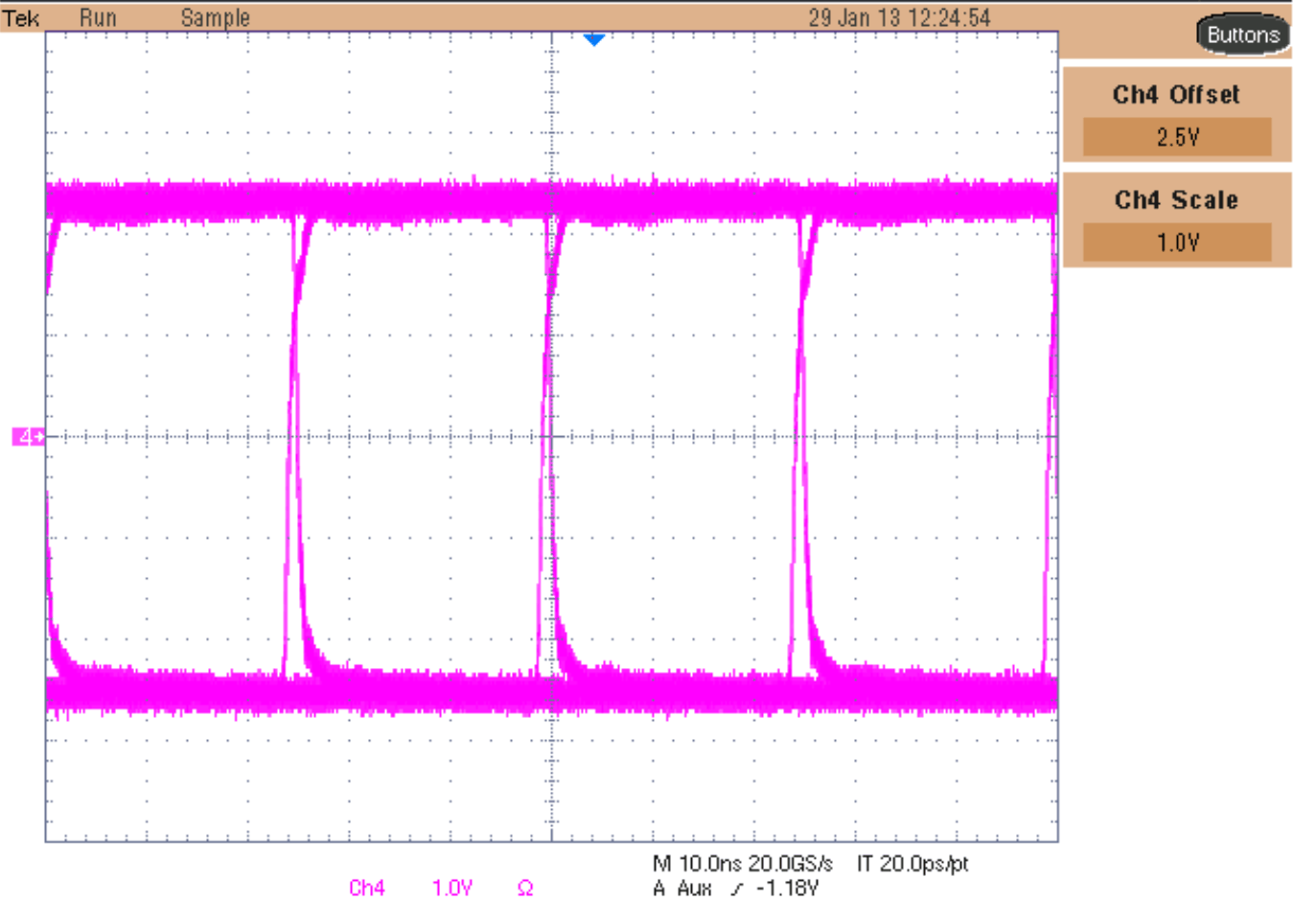
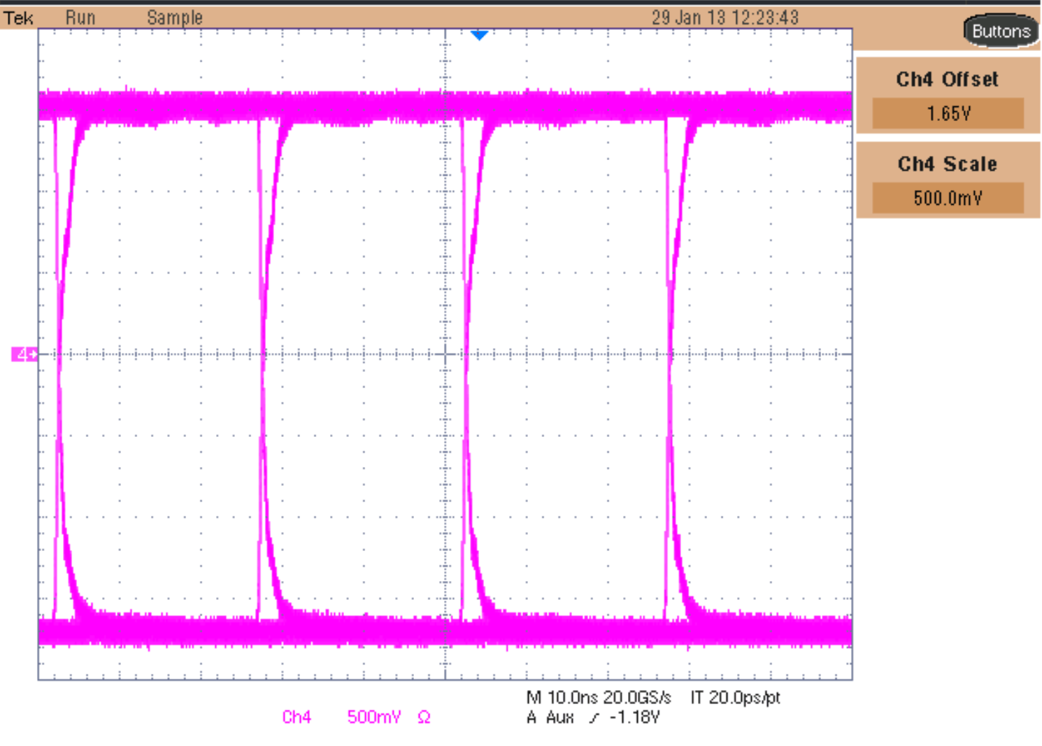
9.2.2.3 Application Curves
See previous Application Curves.