SNVS952F December 2012 – May 2021 LM25019
PRODUCTION DATA
- 1 Features
- 2 Applications
- 3 Description
- 4 Revision History
- 5 Pin Configuration and Functions
- 6 Specifications
-
7 Detailed Description
- 7.1 Overview
- 7.2 Functional Block Diagram
- 7.3
Feature Description
- 7.3.1 Control Overview
- 7.3.2 VCC Regulator
- 7.3.3 Regulation Comparator
- 7.3.4 Overvoltage Comparator
- 7.3.5 On-Time Generator
- 7.3.6 Current Limit
- 7.3.7 N-Channel Buck Switch and Driver
- 7.3.8 Synchronous Rectifier
- 7.3.9 Undervoltage Detector
- 7.3.10 Thermal Protection
- 7.3.11 Ripple Configuration
- 7.3.12 Soft Start
- 7.4 Device Functional Modes
- 8 Application and Implementation
- 9 Power Supply Recommendations
- 10Layout
- 11Device and Documentation Support
- 12Mechanical, Packaging, and Orderable Information
Package Options
Mechanical Data (Package|Pins)
Thermal pad, mechanical data (Package|Pins)
- DDA|8
Orderable Information
8.2.2.8 UVLO Resistors
The UVLO resistors RUV1 and RUV2 set the UVLO threshold and hysteresis according to Equation 18 and Equation 19.
Equation 18. 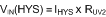
Equation 19. 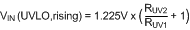
where
- IHYS = 20 μA
Selecting UVLO hysteresis of 2.5 V and UVLO rising threshold of 12 V results in RUV1 = 14.53 kΩ and
RUV2 = 125 kΩ. Selecting a standard value of RUV1 = R7 = 14 kΩ and RUV2 = R5 = 127 kΩ results in UVLO thresholds and hysteresis of 12.5 V to 2.5 V, respectively.