SNVS952F December 2012 – May 2021 LM25019
PRODUCTION DATA
- 1 Features
- 2 Applications
- 3 Description
- 4 Revision History
- 5 Pin Configuration and Functions
- 6 Specifications
-
7 Detailed Description
- 7.1 Overview
- 7.2 Functional Block Diagram
- 7.3
Feature Description
- 7.3.1 Control Overview
- 7.3.2 VCC Regulator
- 7.3.3 Regulation Comparator
- 7.3.4 Overvoltage Comparator
- 7.3.5 On-Time Generator
- 7.3.6 Current Limit
- 7.3.7 N-Channel Buck Switch and Driver
- 7.3.8 Synchronous Rectifier
- 7.3.9 Undervoltage Detector
- 7.3.10 Thermal Protection
- 7.3.11 Ripple Configuration
- 7.3.12 Soft Start
- 7.4 Device Functional Modes
- 8 Application and Implementation
- 9 Power Supply Recommendations
- 10Layout
- 11Device and Documentation Support
- 12Mechanical, Packaging, and Orderable Information
Package Options
Mechanical Data (Package|Pins)
Thermal pad, mechanical data (Package|Pins)
- DDA|8
Orderable Information
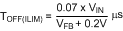
7.3.6 Current Limit
The LM25019 device contains an intelligent current limit off-timer. If the current in the buck switch exceeds
240 mA, the present cycle is immediately terminated, and a nonresetable off-timer is initiated. The length of off-time is controlled by the FB voltage and the input voltage VIN. As an example, when FB = 0 V and VIN = 48 V, the maximum off-time is set to 16 μs. This condition occurs when the output is shorted, and during the initial part of start-up. This amount of time ensures safe short circuit operation up to the maximum input voltage of 48 V.
In cases of overload where the FB voltage is above zero volts (not a short circuit), the current limit off-time is reduced. Reducing the off-time during less severe overloads reduces the amount of foldback, recovery time, and start-up time. The off-time is calculated from Equation 4.
The current limit protection feature is peak limited. The maximum average output is less than the peak.