SNVS509F April 2007 – November 2023 LM25116
PRODUCTION DATA
- 1
- 1 Features
- 2 Applications
- 3 Description
- 4 Pin Configuration and Functions
- 5 Specifications
- 6 Detailed Description
-
7 Application and Implementation
- 7.1 Application Information
- 7.2
Typical Application
- 7.2.1 Design Requirements
- 7.2.2
Detailed Design Procedure
- 7.2.2.1 Timing Resistor
- 7.2.2.2 Output Inductor
- 7.2.2.3 Current Sense Resistor
- 7.2.2.4 Ramp Capacitor
- 7.2.2.5 Output Capacitors
- 7.2.2.6 Input Capacitors
- 7.2.2.7 VCC Capacitor
- 7.2.2.8 Bootstrap Capacitor
- 7.2.2.9 Soft Start Capacitor
- 7.2.2.10 Output Voltage Divider
- 7.2.2.11 UVLO Divider
- 7.2.2.12 MOSFETs
- 7.2.2.13 MOSFET Snubber
- 7.2.2.14 Error Amplifier Compensation
- 7.2.2.15 Comprehensive Equations
- 7.2.3 Application Curves
- 7.3 Power Supply Recommendations
- 7.4 Layout
- 8 Device and Documentation Support
- 9 Revision History
- 10Mechanical, Packaging, and Orderable Information
Package Options
Mechanical Data (Package|Pins)
- PWP|20
Thermal pad, mechanical data (Package|Pins)
- PWP|20
Orderable Information
6.4.1 Soft Start and Diode Emulation
The soft start feature allows the regulator to gradually reach the initial steady state operating point, thus reducing start-up stresses and surges. The LM25116 regulates the FB pin to the SS pin voltage or the internal 1.215-V reference, whichever is lower. At the beginning of the soft-start sequence when SS = 0 V, the internal 10-µA soft-start current source gradually increases the voltage of an external soft-start capacitor (CSS) connected to the SS pin resulting in a gradual rise of FB and the output voltage.
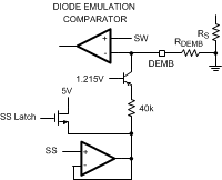
 Figure 6-8 Diode Emulation Control
During this initial charging of CSS to the internal reference voltage, the LM25116 forces diode emulation. That is, the low-side MOSFET turns off for the remainder of a cycle if the sensed inductor current becomes negative. The inductor current is sensed by monitoring the voltage between SW and DEMB. As the SS capacitor continues to charge beyond 1.215 V to 3 V, the DEMB bias current increases from 0 µA up to 40 µA. With the use of an external DEMB resistor (RDEMB), the current sense threshold for diode emulation increases resulting in the gradual transition to synchronous operation. Forcing diode emulation during soft start allows the LM25116 to start up into a prebiased output without unnecessarily discharging the output capacitor. Full synchronous operation is obtained if the DEMB pin is always biased to a higher potential than the SW pin when LO is high. RDEMB = 10 kΩ bias the DEMB pin to 0.45 V minimum, which is adequate for most applications. The DEMB bias potential must always be kept below 2 V. At very light loads with larger values of output inductance and MOSFET capacitance, the switch voltage may fall slowly. If the SW voltage does not fall below the DEMB threshold before the end of the HO fall to LO rise dead time, switching defaults to diode emulation mode. When RDEMB = 0 Ω, the LM25116 always runs in diode emulation.
After SS charges to 3 V the SS latch is set, increasing the DEMB bias current to 65 µA. An amplifier is enabled that regulates SS to 160 mV above the FB voltage. This feature can prevent overshoot of the output voltage in the event the output voltage momentarily dips out of regulation. When a fault is detected (VCC undervoltage, UVLO pin < 1.215 V, or EN = 0 V) the soft-start capacitor is discharged. After the fault condition is no longer present, a new soft-start sequence begins.