SNVS509F April 2007 – November 2023 LM25116
PRODUCTION DATA
- 1
- 1 Features
- 2 Applications
- 3 Description
- 4 Pin Configuration and Functions
- 5 Specifications
- 6 Detailed Description
-
7 Application and Implementation
- 7.1 Application Information
- 7.2
Typical Application
- 7.2.1 Design Requirements
- 7.2.2
Detailed Design Procedure
- 7.2.2.1 Timing Resistor
- 7.2.2.2 Output Inductor
- 7.2.2.3 Current Sense Resistor
- 7.2.2.4 Ramp Capacitor
- 7.2.2.5 Output Capacitors
- 7.2.2.6 Input Capacitors
- 7.2.2.7 VCC Capacitor
- 7.2.2.8 Bootstrap Capacitor
- 7.2.2.9 Soft Start Capacitor
- 7.2.2.10 Output Voltage Divider
- 7.2.2.11 UVLO Divider
- 7.2.2.12 MOSFETs
- 7.2.2.13 MOSFET Snubber
- 7.2.2.14 Error Amplifier Compensation
- 7.2.2.15 Comprehensive Equations
- 7.2.3 Application Curves
- 7.3 Power Supply Recommendations
- 7.4 Layout
- 8 Device and Documentation Support
- 9 Revision History
- 10Mechanical, Packaging, and Orderable Information
Package Options
Mechanical Data (Package|Pins)
- PWP|20
Thermal pad, mechanical data (Package|Pins)
- PWP|20
Orderable Information
7.2.2.11 UVLO Divider
A voltage divider and filter can be connected to the UVLO pin to set a minimum operating voltage VIN(MIN) for the regulator. If this feature is required, the following procedure is used to determine appropriate resistor values for RUV2, RUV1 and CFT.
- RUV2 must be large enough such that in the event of a current limit, the internal UVLO switch can pull UVLO < 200 mV. This can be ensured if: RUV2 > 500 × VIN(MAX), where VIN(MAX) is the maximum input voltage and RUV2 is in ohms.
- With an appropriate value for RUV2, RUV1 can be selected using Equation 25.
Equation 25.
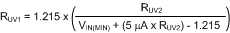
where
- VIN(MIN) is the desired shutdown voltage
- Capacitor CFT provides filtering for the divider and determines the off-time of the hiccup duty cycle during current limit. When CFT is used in conjunction with the voltage divider, a diode across the top resistor must be used to discharge CFT in the event of an input undervoltage condition in Equation 26.
Equation 26.
If undervoltage shutdown is not required, RUV1 and RUV2 can be eliminated and the off-time becomes Equation 27.

The voltage at the UVLO pin must never exceed 16 V when using an external setpoint divider. It may be necessary to clamp the UVLO pin at high input voltages. For the design example, RUV2 = 102 kΩ and
RUV1 = 21 kΩ for a shutdown voltage of 6.6 V. If sustained short-circuit protection is required, CFT ≥ 1 µF limits the short-circuit power dissipation. D2 may be installed when using CFT with RUV1 and RUV2.