SNVS770I June 1999 – January 2015 LM2941 , LM2941C
PRODUCTION DATA.
- 1 Features
- 2 Applications
- 3 Description
- 4 Revision History
- 5 Pin Configuration and Functions
- 6 Specifications
- 7 Detailed Description
- 8 Application and Implementation
- 9 Power Supply Recommendations
- 10Layout
- 11Device and Documentation Support
- 12Mechanical, Packaging, and Orderable Information
Package Options
Refer to the PDF data sheet for device specific package drawings
Mechanical Data (Package|Pins)
- NDH|5
- NGN|8
- KTT|5
- KC|5
Thermal pad, mechanical data (Package|Pins)
- KTT|5
Orderable Information
8 Application and Implementation
NOTE
Information in the following applications sections is not part of the TI component specification, and TI does not warrant its accuracy or completeness. TI’s customers are responsible for determining suitability of components for their purposes. Customers should validate and test their design implementation to confirm system functionality.
8.1 Application Information
Figure 18 shows the typical application circuit for the LM2941. The output capacitor, COUT, must have a capacitance value of at least 22 µF with an equivalent series resistance (ESR) of at least 100 mΩ, but no more than 1 Ω. The minimum capacitance value and the ESR requirements apply across the entire expected operating ambient temperature range.
8.2 Typical Application
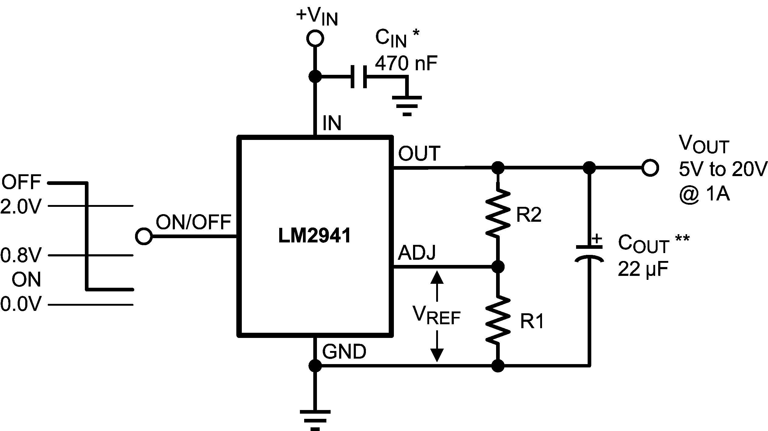
Note: Using 1 kΩ for R1 will ensure that the bias current error from the adjust pin will be negligible. Do not bypass R1 or R2. This will lead to instabilities.
* Required if regulator is located far from power supply filter.
** COUT must be at least 22 μF to maintain stability. May be increased without bound to maintain regulation during transients. Locate as close as possible to the regulator. This capacitor must be rated over the same operating temperature range as the regulator and the ESR is critical.
8.2.1 Design Requirements
| DESIGN PARAMETER | EXAMPLE VALUE |
|---|---|
| Input voltage range | 10 V to 26 V |
| Output voltage | 15 V |
| Output current range | 5 mA to 1 A |
| Input capacitor value | 0.47 µF |
| Output capacitor value | 22 µF minimum |
| Output capacitor ESR range | 100 mΩ to 1 Ω |
8.2.2 Detailed Design Procedure
8.2.2.1 Output Capacitor
A tantalum capacitor with a minimum capacitance value of 22 μF, and ESR in the range of 0.01 Ω to 5 Ω, is required at the output pin for loop stability. It must be located less than 1 cm from the device. There is no limitation on any additional capacitance.
Alternately, a high quality X5R/X7R 22 μF ceramic capacitor may be used for the output capacitor only if an appropriate value of series resistance is added to simulate the ESR requirement. The ceramic capacitor selection must include an appropriate voltage de-rating of the capacitance value due to the applied output voltage. The series resistor (for ESR simulation) should be in the range of 0.1 Ω to 1 Ω.
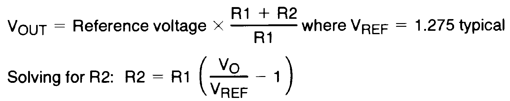
8.2.2.2 Setting the Output Voltage
The output voltage range is 5 V to 20 V and is set by the two external resistors, R1 and R2. See the Figure 18. The output voltage is given by the formula:
where
- VREF is typically 1.275 V
Using 1 kΩ for R1 will ensure that the bias current error of the adjust pin will be negligible. Using a R1 value higher than 10 kΩ may cause the output voltage to shift across temperature due to variations in the adjust pin bias current.
Calculating the upper resistor (R2) value of the pair when the lower resistor (R1) value is known is accomplished with the following formula:
The resistors used for R1 and R2 should be high quality, tight tolerance, and with matching temperature coefficients. It is important to remember that, although the value of VREF is ensured, the final value of VOUT is not. The use of low quality resistors for R1 and R2 can easily produce a VOUT value that is unacceptable.
8.2.3 Application Curves
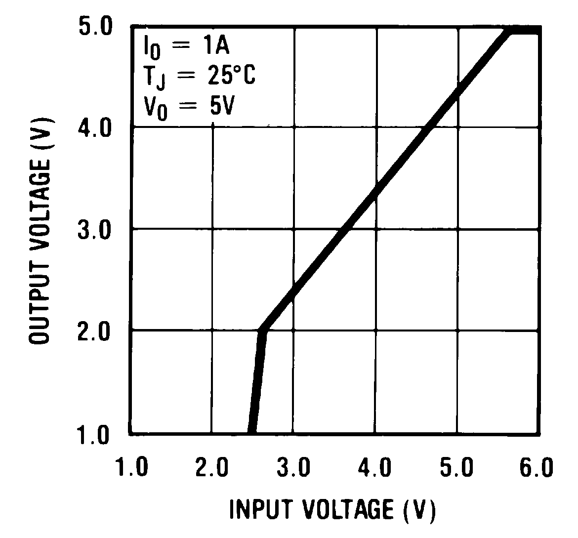 Figure 19. Low Voltage Behavior
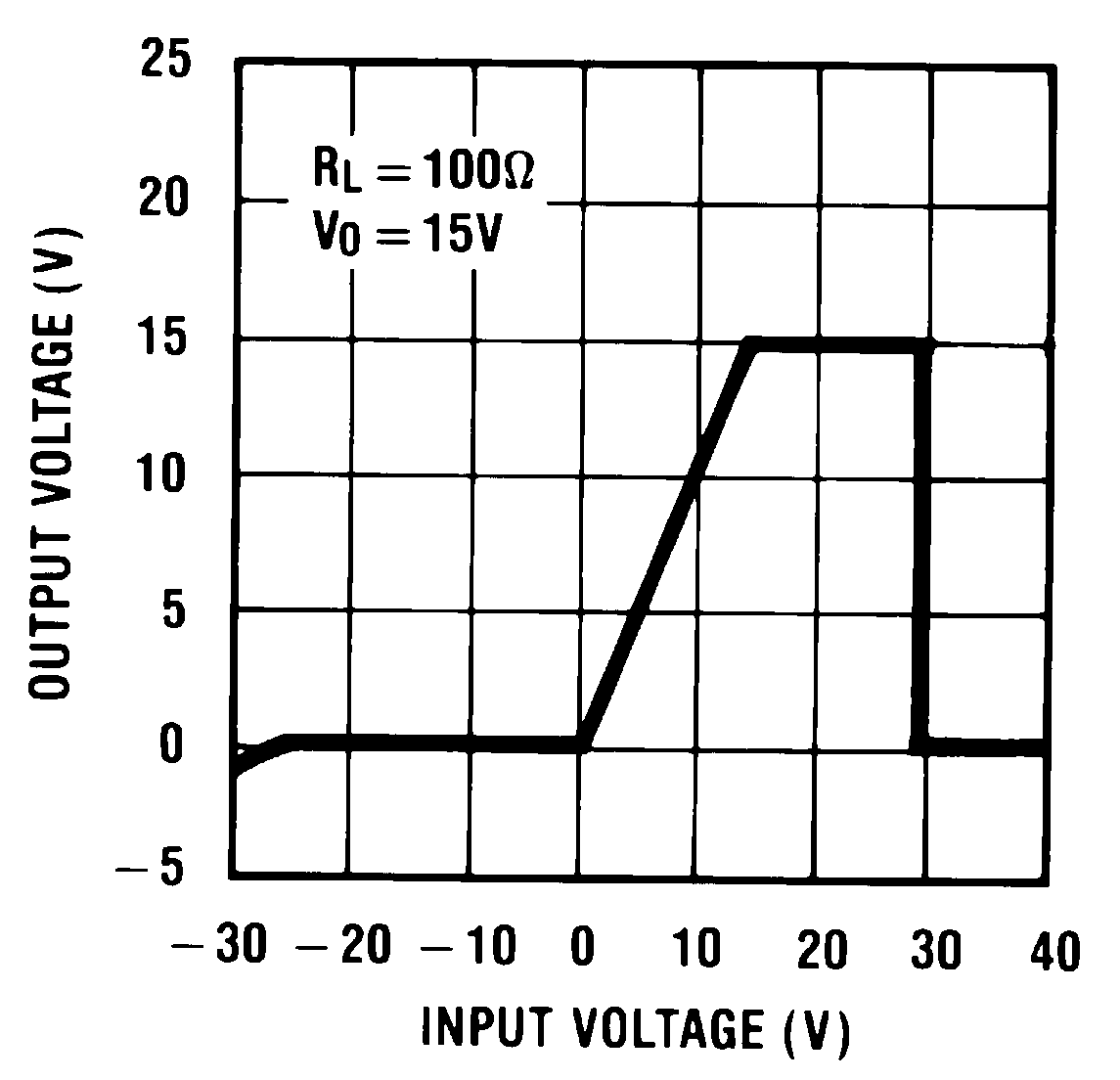 Figure 20. Output at Voltage Extremes