SNVS770I June 1999 – January 2015 LM2941 , LM2941C
PRODUCTION DATA.
- 1 Features
- 2 Applications
- 3 Description
- 4 Revision History
- 5 Pin Configuration and Functions
- 6 Specifications
- 7 Detailed Description
- 8 Application and Implementation
- 9 Power Supply Recommendations
- 10Layout
- 11Device and Documentation Support
- 12Mechanical, Packaging, and Orderable Information
Package Options
Refer to the PDF data sheet for device specific package drawings
Mechanical Data (Package|Pins)
- NDH|5
- NGN|8
- KTT|5
- KC|5
Thermal pad, mechanical data (Package|Pins)
- KTT|5
Orderable Information
7 Detailed Description
7.1 Overview
The LM2941 positive voltage regulator features the ability to source 1 A of output current with a dropout voltage of typically 0.5 V and a maximum of 1 V over the entire temperature range. Furthermore, a quiescent current reduction circuit has been included which reduces the ground current when the differential between the input voltage and the output voltage exceeds approximately 3 V. The quiescent current with 1 A of output current and an input-output differential of 5 V is therefore only 30 mA. Higher quiescent currents only exist when the regulator is in the dropout mode (VIN – VOUT ≤ 3 V).
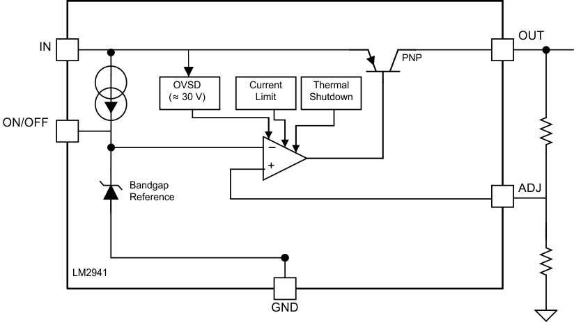
7.2 Functional Block Diagram
7.3 Feature Description
7.3.1 Short-Circuit Current Limit
The internal current limit circuit is used to protect the LDO against high-load current faults or shorting events. The LDO is not designed to operate in a steady-state current limit. During a current-limit event, the LDO sources constant current. Therefore, the output voltage falls when load impedance decreases. Note also that if a current limit occurs and the resulting output voltage is low, excessive power may be dissipated across the LDO, resulting a thermal shutdown of the output.
7.3.2 Overvoltage Shutdown (OVSD)
Input voltage greater than typically 30 V will cause the LM2941 output to be disabled. When operating with the input voltage greater than the maximum recommended input voltage of 26 V, the device performance is not ensured. Continuous operation with the input voltage greater than the maximum recommended input voltage is discouraged.
7.3.3 Thermal Shutdown (TSD)
The LM2941 contains the thermal shutdown circuitry to turn off the output when excessive heat is dissipated in the LDO. The internal protection circuitry of the LM2941 is designed to protect against thermal overload conditions. The TSD circuitry is not intended to replace proper heat sinking. Continuously running the device into thermal shutdown degrades its reliability as the junction temperature will be exceeding the absolute maximum junction temperature rating.
7.3.4 Thermal Overload Protection
The LM2941 incorporates a linear form of thermal protection that limits the junction temperature (TJ) to typically 155°C.
Should the LM2941 see a fault condition that results in excessive power dissipation and the junction temperature approaches 155°C, the device will respond by reducing the output current (which reduces the power dissipation) to hold the junction temperature at 155°C.
Thermal Overload protection is not an ensured operating condition. Operating at, or near to, the thermal overload condition for any extended period of time is not encouraged, or recommended, as this may shorten the lifetime of the device.
7.4 Device Functional Modes
7.4.1 Operation With ON/OFF Control
The ON/OFF pin has no internal pull-up or pull-down to establish a default condition and, as a result, this pin must be terminated externally, either actively or passively. The ON/OFF pin requires a low level to enable the output, and a high level to disable the output. To ensure reliable operation, the ON/OFF pin voltage must rise above the maximum ON/OFF(OFF) voltage threshold (2 V) to disable the output, and must fall below the minimum ON/OFF(ON) voltage threshold (0.8 V) to enable the output. If the ON/OFF function is not needed this pin can be connected directly to Ground. If the ON/OFF pin is being pulled to a high state through a series resistor, an allowance must be made for the ON/OFF pin current that will cause a voltage drop across the pull-up resistor