SNVS974B April 2013 – October 2015 LM3630A
PRODUCTION DATA.
- 1 Features
- 2 Applications
- 3 Description
- 4 Revision History
- 5 Pin Configuration and Functions
- 6 Specifications
-
7 Detailed Description
- 7.1 Overview
- 7.2 Functional Block Diagram
- 7.3
Feature Description
- 7.3.1
Operation
- 7.3.1.1 Control Bank Mapping
- 7.3.1.2 PWM Input Polaritiy
- 7.3.1.3 HWEN Input
- 7.3.1.4 SEL Input
- 7.3.1.5 INTN Output
- 7.3.1.6 Boost Converter
- 7.3.1.7 Boost Switching Frequency Select
- 7.3.1.8 Adaptive Headroom
- 7.3.1.9 Current Sinks
- 7.3.1.10 Current String Biasing
- 7.3.1.11 Full-Scale LED Current
- 7.3.1.12 Brightness Register
- 7.3.1.13 Exponential Mapping
- 7.3.1.14 Linear Mapping
- 7.3.2 Test Features
- 7.3.3 Fault Flags/Protection Features
- 7.3.4 Initialization Timing
- 7.3.1
Operation
- 7.4 Device Functional Modes
- 7.5 Programming
- 7.6 Register Maps
- 8 Application and Implementation
- 9 Power Supply Recommendations
- 10Layout
- 11Device and Documentation Support
- 12Mechanical, Packaging, and Orderable Information
Package Options
Mechanical Data (Package|Pins)
- YFQ|12
Thermal pad, mechanical data (Package|Pins)
Orderable Information
8 Application and Implementation
NOTE
Information in the following applications sections is not part of the TI component specification, and TI does not warrant its accuracy or completeness. TI’s customers are responsible for determining suitability of components for their purposes. Customers should validate and test their design implementation to confirm system functionality.
8.1 Application Information
The LM3630A is a dual-channel backlight driver. The device has 5-bit full-scale current programmability (5 mA to 30 mA) and for every full-scale current there is 8 bits of LED current adjustment from 0 to IFULL_SCALE. Both current sinks can be independently controlled via two separate full-scale current registers and two separate 8-bit brightness registers, or can be made to track together via a single brightness register.
8.2 Typical Application
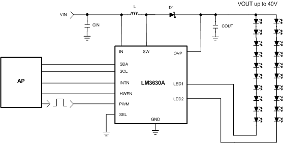 Figure 87. LM3630A Typical Application
8.2.1 Design Requirements
For typical white LED applications, use the parameters listed in Table 21.
Table 21. Design Parameters
| DESIGN PARAMETER | EXAMPLE VALUE |
|---|---|
| Minimum input voltage | 2.3 V |
| Minimum output voltage | VIN |
| Output current | 28.5 mA per channel |
| Switching frequency | 500 kHz or 1 MHz |
8.2.2 Detailed Design Procedure
8.2.2.1 Inductor Selection
The LM3630A is designed to work with a 10-µH to 22-µH inductor. When selecting the inductor, ensure that the saturation rating for the inductor is high enough to accommodate the peak inductor current. Equation 4 calculates the peak inductor current based upon LED current, VIN, VOUT, and efficiency.

where:

When choosing L, the inductance value must also be large enough so that the peak inductor current is kept below the LM3630A device's switch current limit. This forces a lower limit on L given by Equation 6.

ISW_MAX is given in Electrical Characteristics, efficiency (η) is shown in theTypical Characteristics, and ƒSW is typically 500 kHz or 1 MHz.
Table 22. Inductors
| MANUFACTURER | PART NUMBER | VALUE | SIZE | CURRENT RATING | DC RESISTANCE |
|---|---|---|---|---|---|
| TDK | VLF4014ST-100M1R0 | 10 µH | 3.8 mm × 3.6 mm × 1.4 mm | 1A | 0.22 Ω |
| TDK | VLF302512MT-220M | 22 µH | 3 mm × 2.5 mm × 1.2 mm | 0.43A | 0.583 Ω |
8.2.2.2 Maximum Power Output
The LM3630A device's maximum output power is governed by two factors: the peak current limit (ICL = 1.2 A maximum), and the maximum output voltage (VOVP = 40 V minimum). When the application causes either of these limits to be reached, it is possible that the proper current regulation and matching between LED current strings may not be met.
In the case of a peak current limited situation, when the peak of the inductor current hits the LM3630A device's current limit the NFET switch turns off for the remainder of the switching period. If this happens, each switching cycle the LM3630A begins to regulate the peak of the inductor current instead of the headroom across the current sinks. This can result in the dropout of the feedback-enabled current sinks and the current dropping below its programmed level.
The peak current in a boost converter is dependent on the value of the inductor, total LED current (IOUT), the output voltage (VOUT) (which is the highest voltage LED string + 0.3 V regulated headroom voltage), the input voltage VIN, and the efficiency (Output Power/Input Power). Additionally, the peak current is different depending on whether the inductor current is continuous during the entire switching period (CCM) or discontinuous (DCM) where it goes to 0 before the switching period ends.
For CCM the peak inductor current is given by:

For DCM the peak inductor current is given by:

To determine which mode the circuit is operating in (CCM or DCM), a calculation must be done to test whether the inductor current ripple is less than the anticipated input current (IIN). If ΔIL is < IIN, the device operates in CCM. If ΔIL is > IIN then the device is operating in DCM.

Typically at currents high enough to reach the LM3630A device's peak current limit, the device is operating in CCM.
Application Curves show the output current and output voltage derating for a 10-µH and a 22-µH inductor, at switch frequencies of 500 kHz and 1 MHz. A 10-µH inductor is typically a smaller device with lower on resistance, but the peak currents are higher. A 22-µH inductor provides for lower peak currents, but to match the DC resistance of a 10 µH requires a larger-sized device.
8.2.3 Application Curves
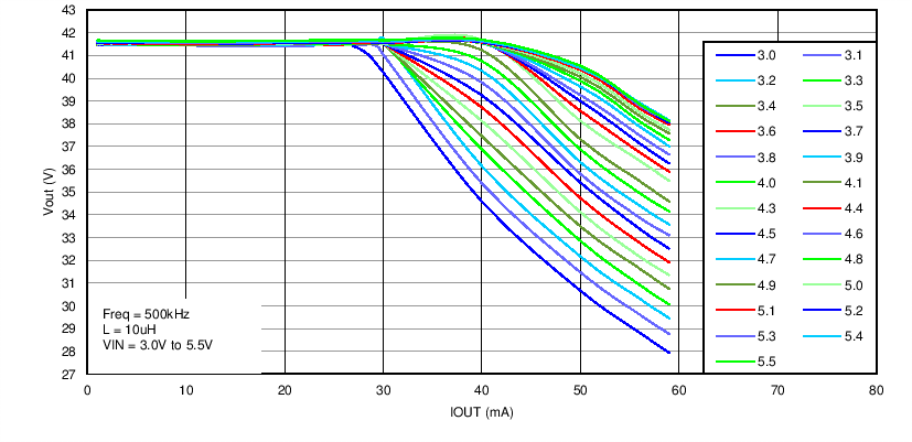
| Frequency = 500 kHz | L = 10 µH |
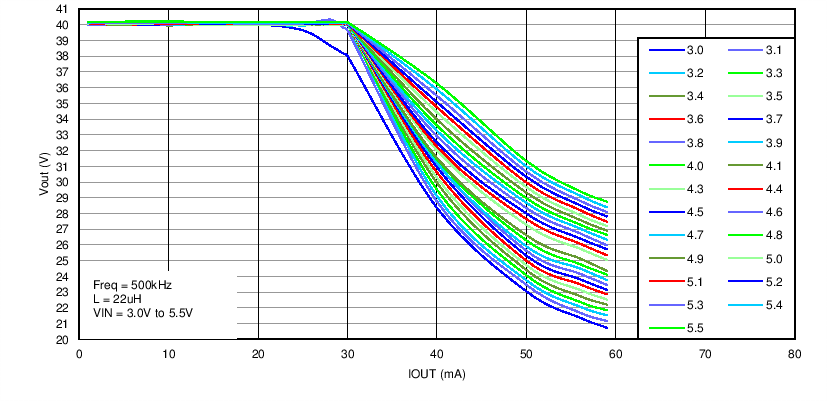
| Frequency = 500 kHz | L = 22 µH |
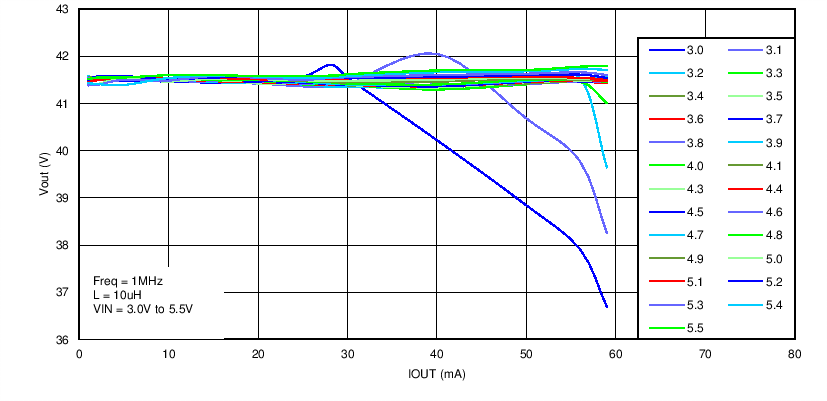
| Frequency = 1 MHz | L = 10 µH |
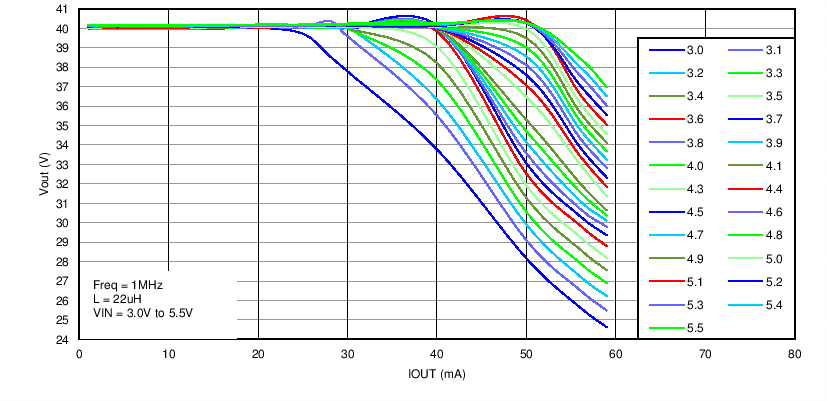
| Frequency = 1 MHz | L = 22 µH |
8.3 Initialization Setup
8.3.1 Recommended Initialization Sequence
The recommended initialization sequence for the device registers is as follows:
- Set Filter Strength register (offset = 50h) to 03h.
- Set Configuration register (offset = 01h) to enable the PWM and the feedback for Bank A; for example, writing 09h to the Configuration register, enables PWM and feedback for Bank A. Note the Bank B PWM and feedback need to be configured if Bank B is used, otherwise disable the Bank B feedback by clearing bit 4 and disable the Bank B PWM by clearing bit 1.
- Configure the Boost Control register (offset = 02h) to select the OVP, OCP and FMODE. For example, writing 78h to the Boost Control register sets OVP to 40 V, OCP to 1.2 A and FMODE to 500 kHz.
- Set the full scale LED current for Bank A and Bank B (if used), by writing to the Current A (offset = 05h), and Current B(offset = 06) registers. For example, writing 14h to the Current A register selects a full scale LED current of 20 mA for Bank A.
- Set the PWM Sampler Hysteresis to 2 codes by setting Bit 7 of the Current A register. Set the PWM Sampler Lower Bound code to 6 by clearing Bit 6 of the Current A register. Note these settings apply to both Bank A and Bank B. If only Bank B is used, these setting are still necessary when PWM is enabled.
- Select the current control and enable or disable the LED Bank A and/or B by writing to Control register(offset = 00h). For example, writing 14h to the Control register select linear current control and enables Bank A.
- Set the LED brightness by writing to Brightness A (offset = 03h) and Brightness B (Offset = 04h) registers. For example, writing FFh to Brightness A sets the LED current to 20 mA, with the Current A register set to 14h, and the PWM input is high.