SNVS974B April 2013 – October 2015 LM3630A
PRODUCTION DATA.
- 1 Features
- 2 Applications
- 3 Description
- 4 Revision History
- 5 Pin Configuration and Functions
- 6 Specifications
-
7 Detailed Description
- 7.1 Overview
- 7.2 Functional Block Diagram
- 7.3
Feature Description
- 7.3.1
Operation
- 7.3.1.1 Control Bank Mapping
- 7.3.1.2 PWM Input Polaritiy
- 7.3.1.3 HWEN Input
- 7.3.1.4 SEL Input
- 7.3.1.5 INTN Output
- 7.3.1.6 Boost Converter
- 7.3.1.7 Boost Switching Frequency Select
- 7.3.1.8 Adaptive Headroom
- 7.3.1.9 Current Sinks
- 7.3.1.10 Current String Biasing
- 7.3.1.11 Full-Scale LED Current
- 7.3.1.12 Brightness Register
- 7.3.1.13 Exponential Mapping
- 7.3.1.14 Linear Mapping
- 7.3.2 Test Features
- 7.3.3 Fault Flags/Protection Features
- 7.3.4 Initialization Timing
- 7.3.1
Operation
- 7.4 Device Functional Modes
- 7.5 Programming
- 7.6 Register Maps
- 8 Application and Implementation
- 9 Power Supply Recommendations
- 10Layout
- 11Device and Documentation Support
- 12Mechanical, Packaging, and Orderable Information
Package Options
Mechanical Data (Package|Pins)
- YFQ|12
Thermal pad, mechanical data (Package|Pins)
Orderable Information
7 Detailed Description
7.1 Overview
The LM3630A provides the power for two high-voltage LED strings (up to 40 V at 28.5 mA each). The two high-voltage LED strings are powered from an integrated asynchronous boost converter. The device is programmable over an I2C-compatible interface. Additional features include a PWM input for content adjustable brightness control, programmable switching frequency, and programmable overvoltage protection (OVP).
7.2 Functional Block Diagram
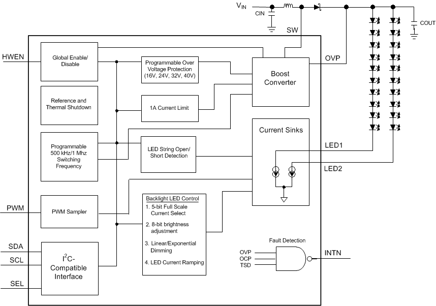
7.3 Feature Description
7.3.1 Operation
7.3.1.1 Control Bank Mapping
Control of the LM3630A device current sinks is not done directly, but through the programming of Control Banks. The current sinks are then assigned to the programmed Control Bank (see Figure 72). Both current sinks can be assigned to Control Bank A or LED1 can use Control Bank A while LED2 uses Control Bank B. Assigning LED1 to Control Bank A and LED2 to Control Bank B allows for better LED current matching. Assigning each current sink to different control banks allows for each current sink to be programmed with a different current or have the PWM input control a specific current sink.
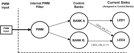 Figure 72. Control Diagram
Table 1. Bank Configuration Examples: Register Values
| REGISTERS TO PROGRAM | ILED1 on A, ILED2 ON B WITH PWM DIMMING(1) | ILED1 AND ILED2 ON A WITH PWM DIMMING | ILED1 ON A WITH PWM ILED2 ON B NO PWM |
|---|---|---|---|
| Control | 1EH linear or 06h exp | 15h linear or 05h exp | 1EH linear or 06h exp |
| Configuration | 1Bh | 09h | 19h |
| Brightness A | used for A | used for both | used for A |
| Brightness B | used for B | not used | used for B (A and B do not have to be equal) |
7.3.1.2 PWM Input Polaritiy
The PWM Input can be set for active high (default) or active low polarity. With active low polarity the LED current is a function of the negative duty cycle at PWM.
7.3.1.3 HWEN Input
HWEN is the global hardware enable to the LM3630A. HWEN must be pulled high to enable the device. HWEN is a high-impedance input so it cannot be left floating. When HWEN is pulled low the LM3630A is placed in shutdown and all the registers are reset to their default state.
7.3.1.4 SEL Input
SEL is the select pin for the serial bus device address. When this pin is connected to ground, the seven-bit device address is 36H. When this pin is tied to the VIN power rail, the device address is 38H.
7.3.1.5 INTN Output
The INTN pin is an open-drain active-low output signal which indicates detected faults. The signal asserts low when either OCP, OVP, or TSD is detected by the LED driver. The Interrupt Enable register must be set to connect these faults to the INTN pin.
7.3.1.6 Boost Converter
The high-voltage boost converter provides power for the two current sinks (ILED1 and ILED2). The boost circuit operates using a 10-μH to 22-μH inductor and a 1-μF output capacitor. The selectable 500-kHz or 1-MHz switching frequency allows for the use of small external components and provides for high boost converter efficiency. Both LED1 and LED2 feature an adaptive voltage regulation scheme where the feedback point (LED1 or LED2) is regulated to a minimum of 300 mV. When there are different voltage requirements in both high-voltage LED strings, because of different programmed voltages or string mismatch, the LM3630A regulates the feedback point of the highest voltage string to 300 mV and drop the excess voltage of the lower voltage string across the lower strings current sink.
7.3.1.7 Boost Switching Frequency Select
The LM3630A’s boost converter can have a 500-kHz or 1-MHz switching frequency. For a 500-kHz switching frequency the inductor value must be between 10 μH and 22 μH. For the 1-MHz switching frequency the inductor can be between 10 μH and 22 μH. Additionally, there is a Frequency Shift bit which offsets the frequency approximately 10%. For the 500 kHz setting, shift = 0. The boost frequency is shifted to 560 kHz when Shift = 1. For the 1-MHz setting, Shift = 0. The boost frequency is shifted to 1120 kHz when shift = 1.
7.3.1.8 Adaptive Headroom
Reference Figure 73 and Figure 74 for the following description.
The adaptive headroom circuit controls the boost output voltage to provide the minimal headroom voltage necessary for the current sinks to provide the specified ILED current. The headroom voltage is fed back to the Error Amplifier to dynamically adjust the Boost output voltage. The error amplifier's reference voltage is adjusted as the brightness level is changed, because the currents sinks require less headroom at lower ILED currents than at higher ILED currents. Note that the VHR Min block dynamically selects the LED string that requires the higher boost voltage to maintain the ILED current; this string has the lower headroom voltage. In Figure 74 this is LED string 2. The headroom voltage on LED string 1 is higher, but this is due to LED string 2 have an overall higher forward voltage than LED string 1. LED strings that have closely matched forward voltages have closely matched headroom voltages and better overall efficiency.
In a single string LED configuration the Feedback enable must be enabled for only that string (LED1 or LED2). The adaptive headroom circuit is control by that single string. In a two string LED configuration the Feedback enable must be enabled for both strings (LED1 and LED2). The VHR Min block then dynamically selects the LED string to control the adaptive headroom circuit.
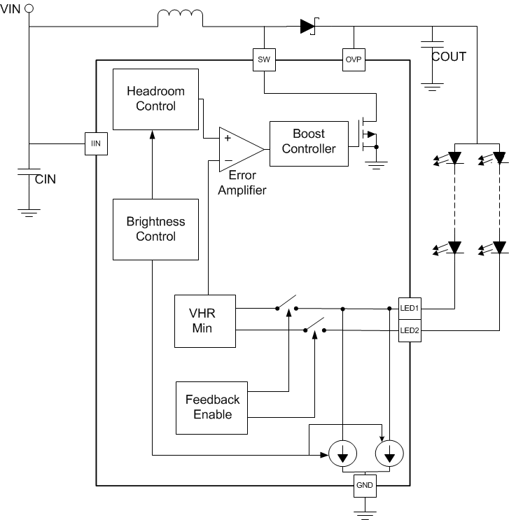 Figure 73. Adaptive Headroom Block Diagram
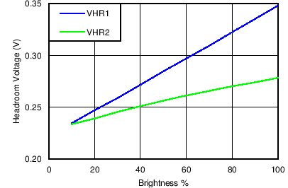 Figure 74. Typical Headroom Voltage Curve
7.3.1.9 Current Sinks
LED1 and LED2 control the current up to a 40-V LED string voltage. Each current sink has 5-bit full-scale current programmability and 8-bit brightness control. Either current sink has its current set through a dedicated brightness register and can additionally be controlled via the PWM input.
7.3.1.10 Current String Biasing
Each current string can be powered from the LM3630A device’s boost or from an external source. When powered from an external source the feedback input for either current sink can be disabled in the Configuration Register so it no longer controls the boost output voltage.
7.3.1.11 Full-Scale LED Current
The LM3630A device’s full-scale current is programmable with 32 different full-scale levels. The full-scale current is the LED current in the control bank when the brightness code is at max code (0xFF). The 5-bit full-scale current vs code is given by Equation 1:
With a maximum full-scale current of 28.5 mA.
7.3.1.12 Brightness Register
Each control bank has its own 8-bit brightness register. The brightness register code and the full-scale current setting determine the LED current depending on the programmed mapping mode.
7.3.1.13 Exponential Mapping
In exponential mapping mode the brightness code to backlight current transfer function is given by Equation 2:

where
- ILED_FULLSCALE is the full-scale LED current setting
- Code is the backlight code in the brightness register
- DPWM is the PWM input duty cycle
Figure 75 and Figure 76 show the approximate backlight code to LED current response using exponential mapping mode. Figure 75 shows the response with a linear Y axis, and Figure 76 shows the response with a logarithmic Y axis. In exponential mapping mode the current ramp (either up or down) appears to the human eye as a more uniform transition then the linear ramp. This is due to the logarithmic response of the eye.
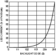 Figure 75. Exponential Mapping Mode (Linear Scale)
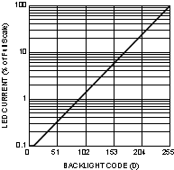 Figure 76. Exponential Mapping Mode (Log Scale)
7.3.1.14 Linear Mapping
In linear mapping mode the brightness code to backlight current has a linear relationship and follows Equation 3:

where
- ILED_FULLSCALE is the full scale LED current setting
- Code is the backlight code in the brightness register
- DPWM is the PWM input duty cycle
Figure 77 shows the backlight code-to-LED current response using linear-mapping mode. The Configuration Register must be set to enable linear mapping.
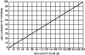 Figure 77. Linear Mapping Mode
7.3.2 Test Features
The LM3630A contains an LED open, an LED short, and overvoltage manufacturing fault detection. This fault detection is designed to be used during the manufacturing process only and not normal operation. These faults do not set the INTN pin.
7.3.2.1 Open LED String (LED1 And LED2)
An open LED string is detected when the voltage at the input to either LED1 or LED2 has fallen below 200 mV, and the boost output voltage has hit the OVP threshold. This test assumes that the LED string that is being detected for an open is being powered from the boost output (Feedback Enabled). For an LED string not connected to the boost output, and connected to another voltage source, the boost output would not trigger the OVP flag. In this case an open LED string would not be detected.
7.3.2.2 Shorted LED String
The LM3630A features an LED short fault flag indicating if either of the LED strings have experienced a short. There are two methods that can trigger a short in the LED strings:
- An LED current sink with feedback enabled, and the difference between OVP input and the LED current sink input voltage goes below 1 V.
- An LED current sink is configured with feedback disabled (not powered from the boost output) and the difference between VIN and the LED current sink input voltage goes below 1 V.
7.3.2.3 Overvoltage Protection (Manufacturing Fault Detection and Shutdown)
The LM3630A provides an overvoltage Protection (OVP) mechanism specifically for manufacturing test where a display may not be connected to the device. The OVP threshold on the LM3630A has 4 different programmable options (16 V, 24 V, 32 V, and 40 V). The manufacturing protection is enabled in the Fault Status register bit 0. When enabled, this feature causes the boost converter to shutdown anytime the selected OVP threshold is exceeded. The OVP_fault bit in the Fault Status register is set to one. The boost converter does not resume operation until the LM3630A is reset with either a write to the Software Reset bit in the Software Reset register or a cycling of the HWEN pin. The reset clears the fault.
7.3.3 Fault Flags/Protection Features
The Interrupt Status register contains the status of the protection circuits of the LM3630A. The corresponding bits are set to one if an OVP, OCP, or TSD event occurs. These faults do set the INTN pin when the corresponding bit is set in the Interrupt Enable register.
7.3.3.1 Overvoltage Protection (Inductive Boost Operation)
The overvoltage protection threshold (OVP) on the LM3630A has 4 different programmable options (16 V, 24 V, 32 V, and 40 V). OVP protects the device and associated circuitry from high voltages in the event the feedback enabled LED string becomes open. During normal operation, the LM3630A device’s inductive boost converter boosts the output up so as to maintain at least 300 mV at the active current sink inputs. When a high-voltage LED string becomes open the feedback mechanism is broken, and the boost converterinadvertently over boosts the output. When the output voltage reaches the OVP threshold the boost converter stops switching, thus allowing the output node to discharge. When the output discharges to VOVP – 1 V the boost converter begins switching again. The OVP sense is at the OVP pin, so this pin must be connected directly to the inductive boost output capacitor’s positive terminal.
For current sinks that have feedback disabled the over voltage sense mechanism is not in place to protect from potential over-voltage conditions. In this situation the application must ensure that the voltage at LED1 or LED2 doesn’t exceed 40 V.
The default setting for OVP is set at 24 V. For applications that require higher than 24 V at the boost output the OVP threshold has to be programmed to a higher level at power up.
7.3.3.2 Current Limit
The switch current limit for the LM3630A device’s inductive boost is set at 1 A. When the current through the NFET switch hits this over current protection threshold (OCP) the device turns the NFET off and the energy of the inductor is discharged into the output capacitor. Switching is then resumed at the next cycle. The current limit protection circuitry can operate continuously each switch cycle. The result is that during high output power conditions the device can continuously run in current limit. Under these conditions the device inductive boost converter stops regulating the headroom voltage across the high voltage current sinks. This results in a drop in the LED current.
7.3.3.3 Thermal Shutdown
The LM3630A contains thermal shutdown protection. In the event the die temperature reaches 140°C, the boost power supply and current sinks shut down until the die temperature drops to typically 125°C.
7.3.4 Initialization Timing
7.3.4.1 Initialization Timing With HWEN Tied to VIN
If the HWEN input is tied to VIN, then the tWAIT time starts when VIN crosses 2.5 V as shown in Figure 78. The initial I2C transaction can occur after the tWAIT time expires. Any I2C transaction during the tWAIT period are NAK'ed.
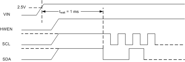 Figure 78. Initialization Timing With HWEN Is Tied to VIN
7.3.4.2 Initialization Timing With HWEN Driven by GPIO
If the HWEN input is driven by a GPIO then the tWAITtime starts when HWEW crosses 1.2 V as shown in Figure 79. The initial I2C transaction can occur after the tWAIT time expires. Any I2C transaction during the tWAIT period are NAK'ed.
 Figure 79. Initialization Timing With HWEN Driven by a GPIO
7.3.4.3 Initialization After Software Reset
The time between the I2C transaction that issues the software reset, and the subsequent I2C transaction (that is, to configure the LM3630A) must be at greater or equal to the tWAIT period of 1 ms. Any I2C transaction during the tWAIT period are NAK'ed.
7.4 Device Functional Modes
7.4.1 LED Current Ramping
7.4.1.1 Start-Up/Shutdown Ramp
The LED current turn on time from 0 to the initial LED current set-point is programmable. Similarly, the LED current shutdown time to 0 is programmable. Both the startup and shutdown times are independently programmable with 8 different levels. The start-up times are independently programmable from the shutdown times, but not independently programmable for each Control bank. For example, programming a start-up or shutdown time, programs the same ramp time for each control bank. The start-up time is used when the device is first enabled to a non-zero brightness value. The shutdown time is used when the brightness value is programmed to zero. If HWEN is used to disable the device, the action is immediate and the Shutdown time is not used. The zero code does take a small amount of time which is approximately 0.5 ms.
Table 2. Start-Up/Shutdown Times
| CODE | START-UP TIME | SHUTDOWN TIME |
|---|---|---|
| 000 | 4 ms | 0 |
| 001 | 261 ms | 261 ms |
| 010 | 522 ms | 522 ms |
| 011 | 1.045 s | 1.045 s |
| 100 | 2.091 s | 2.091 s |
| 101 | 4.182 s | 4.182 s |
| 110 | 8.364 s | 8.364 s |
| 111 | 16.73 s | 16.73 s |
7.4.1.2 Run-Time Ramp
Current ramping from one brightness level to the next is programmable. There are 8 different ramp up times and 8 different ramp down times. The ramp up time is independently programmable from the ramp down time, but not independently programmable for each Control Bank. For example, programming a ramp up time or a ramp down time programs the same ramp time for each control bank. The run time ramps are used whenever the device is enabled with a non-zero brightness value and a new non-zero brightness value is written.
Table 3. LED Current Run Ramp Times
| CODE | RAMP-UP TIME | RAMP-DOWN TIME |
|---|---|---|
| 000 | 0 | 0 |
| 001 | 261 ms | 261 ms |
| 010 | 522 ms | 522 ms |
| 011 | 1.045s | 1.045s |
| 100 | 2.091s | 2.091s |
| 101 | 4.182s | 4.182s |
| 110 | 8.364s | 8.364s |
| 111 | 16.73s | 16.73s |
7.4.2 PWM Operation
 Figure 80. PWM Sampler
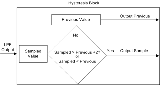 Figure 81. Hysteresis Block (Details)
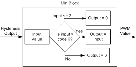 Figure 82. Min Block (Details)
7.4.2.1 PWM Input
The PWM input can be assigned to any control bank. When assigned to a control bank, the programmed current in the control bank also becomes a function of the duty cycle at the PWM input. The PWM input is sampled by a digital circuit which outputs a brightness code that is equivalent to the PWM input duty cycle. The resultant brightness value is a combination of the maximum current setting, the brightness registers, and the equivalent PWM brightness code.
7.4.2.2 PWM Input Frequency
The specified input frequency of the PWM signal is 10 kHz to 80 kHz. The recommended frequency is 30 kHz or greater. The PWM input sampler operates beyond those frequency limits. Performance changes based on the input frequency used. Using frequencies outside the specified range is not recommended. Lower PWM input frequency increases the likelihood that the output of the sampler may change and that a single brightness step may be visible on the screen. This may be visible at low brightness because the step change is large relative to the output level.
7.4.2.3 Recommended Settings
For best performance of the PWM sampler it is recommended to have a PWM input frequency of at least 30 kHz. The Filter Strength (register 50h) must be set to 03h. The Hysteresis 1 bit must be set in register 05h to 1 when setting the maximum current for bank A. For example if max current is 20 mA, register 05h is set to 14h, change that to 94h for 1 bit hysteresis and a smooth min-to-max brightness transition.
7.4.2.4 Adjustments to PWM Sampler
The digital sampler has controls for hysteresis and minimum output brightness which allow the optimization of sampler output. The default hysteresis mode of the PWM sampler requires detecting a two code change in the input to increase brightness. Reducing the hysteresis to change on 1 code allows a smoother brightness transition when the brightness control is swept across the screen in a system. The filter strength bits affect the speed of the output transitions from the PWM sampler. A lower bound to the brightness is enabled by default which limits the minimum output of the PWM sampler to an equivalent code of 6 when the LEDs are turned on. A detected code of 1 is forced to off. A minimum 2% PWM input duty cycle is recommended. Input duty cycles of 1% or less causes delayed off-to-on transitions.
7.4.2.4.1 Filter Strength, Register 50h Bits [1:0]
- Filter Strength controls the amount of sampling cycles that are fed back to the PWM input sampler. A filter strength of 00b allows the output of the PWM sampler to change on every Sample Period. A filter strength of 01b allows the output of the PWM sampler to change every two Sample Periods. A filter strength of 10b allows the output of the PWM sampler to change every four Sample Periods. A filter strength of 11b allows the output of the PWM sampler to change every eight Sample Periods.
- he effect of setting this value to 11b forces the output of the PWM sampler to change less frequently then lower values. The benefit is this reduces the appearance of flicker because the output is slower to change. The negative is that the output is slower to change.
7.4.2.4.2 Hysteresis 1 Bit, Register 05h, Bit 7
- The default setting for the LM3630A has Bit 7 of register 05h is 0b. This requires the detection of a PWM input change that is at least 3 equivalent codes higher than the present code. If this bit is set to 1b, the hysteresis is turned off and the PWM sampler output is allowed to change by 2 code.
- Setting this bit to 1b turns off the 2 code requirement for the PWM sampler output to change. The benefit is that the output change is smoother. The negative is that there may be some PWM input value where the output could change by one code and it might appear as flicker.
7.4.2.4.3 Lower Bound Disable, Register 05h, Bit 6
- The default setting for the LM3630A has Bit 6 of register 05h is 0b. This turns on the lower bound where the minimum output value of the PWM sampler is an equivalent code of 6. If the PWM sampler detects an equivalent code of 0 or 1, the output is 0, and the LEDs are off. If the PWM sampler detects an equivalent code of 2 through 6, a current equal to code 6 is output. Detection of any higher code outputs that code conforming to the rules of hysteresis above.
- Setting Bit 6 of register 05h to 1b can be used to allow the output to be below an equivalent code 6. The output of the PWM sampler matches the input pulse width conforming to the rules of Hysteresis and equivalent codes 1, 2, 3, 4, and 5 are also allowed. The benefit is the output is allowed to go dimmer than in the default mode. The negative is at the low codes of 1 and 2, the LEDs may not turn on or the LEDs may appear to flicker.
- Disabling the Lower Bound (05h Bit 6 = 1b) allows the minimum duty cycle to be detected at 0.35% PWM input duty cycle. At 30-kHz PWM input frequency, the minimum pulse width required to turn on the LEDs is 0.39% × 33 µS = 129 ns. There is no specified tolerance to this value.
7.4.2.5 Minimum TON Pulse Width
The minimum TON pulse width required to produce a non-zero output is dependent upon the LM3630A settings. The default setting of the LM3630A requires a minimum of 0.78% duty cycle for the output to be turned on. Because the lower bound feature is enabled, a value of 0.78% (equivalent brightness code 2) up to 2.35% (equivalent brightness code 6) all produce an output equivalent to brightness code 6. At 30-kHz PWM input frequency, the minimum pulse width required to turn on the LEDs is 0.78% × 33 µS = 260 ns.
Because of the hysteresis on the PWM input, this pulse width may not be sufficient to turn on the LEDs. It is recommended that a minimum pulse width of 2% be used. 2% × 33 µS = 660 ns at 30 kHz input frequency.
Disabling the lower bound as described allows a smaller minimum pulse width.
7.5 Programming
7.5.1 I2C-Compatible Interface
7.5.1.1 Data Validity
The data on SDA line must be stable during the HIGH period of the clock signal (SCL). In other words, state of the data line can only be changed when SCL is LOW.
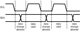 Figure 83. Data Validity Diagram
A pullup resistor between the VIO line of the controller and SDA must be greater than [(VIO – VOL) / 3 mA] to meet the VOL requirement on SDA. Using a larger pullup resistor results in lower switching current with slower edges, while using a smaller pullup results in higher switching currents with faster edges.
7.5.1.2 Start and Stop Conditions
START and STOP conditions classify the beginning and the end of the I2C session. A START condition is defined as SDA signal transitioning from HIGH to LOW while SCL line is HIGH. A STOP condition is defined as the SDA transitioning from LOW to HIGH while SCL is HIGH. The I2C master always generates START and STOP conditions. The I2C bus is considered to be busy after a START condition and free after a STOP condition. During data transmission, the I2C master can generate repeated START conditions. First START and repeated START conditions are equivalent, function-wise.
 Figure 84. Start and Stop Conditions
7.5.1.3 Transferring Data
Every byte put on the SDA line must be eight bits long, with the most significant bit (MSB) transferred first. Each byte of data has to be followed by an acknowledge bit. The acknowledge related clock pulse is generated by the master. The master releases the SDA line (HIGH) during the acknowledge clock pulse. The LM3630A pulls down the SDA line during the 9th clock pulse, signifying an acknowledge. The LM3630A generates an acknowledge after each byte is received.
After the START condition, the I2C master sends a chip address. This address is seven bits long followed by an eighth bit which is a data direction bit (R/W). The LM3630A address is 36h. For the eighth bit, a “0” indicates a WRITE and a “1” indicates a READ. The second byte selects the register to which the data is written. The third byte contains data to write to the selected register.
 Figure 85. I2C-Compatible Chip Address (0x36), SEL = 0
 Figure 86. I2C-Compatible Chip Address (0x38), SEL = 1
7.6 Register Maps
7.6.1 LM3630A I2C Register Map
This table summarizes LM3630A I2C-compatible register usage and shows default register bit values after reset, as programmed by the factory. The following sub-sections provide additional details on the use of individual registers. Register bits which are blank in the following tables are considered undefined. Undefined bits should be ignored on reads and written as zero.
| SLAVE ADDRESS [0x36h for SEL = 0, 0x38h for SEL = 1] |
|||
|---|---|---|---|
| BASE REGISTERS | |||
| REGISTER NAME | ADDRESS | TYPE | DEFAULT RESET VALUES |
| Control | 0x00 | R/W | 0xC0 |
| Configuration | 0x01 | R/W | 0x18 |
| Boost Control | 0x02 | R/W | 0x38 |
| Brightness A | 0x03 | R/W | 0x00 |
| Brightness B | 0x04 | R/W | 0x00 |
| Current A | 0x05 | R/W | 0x1F |
| Current B | 0x06 | R/W | 0x1F |
| On/Off Ramp | 0x07 | R/W | 0x00 |
| Run Ramp | 0x08 | R/W | 0x00 |
| Interrupt Status | 0x09 | R/W | 0x00 |
| Interrupt Enable | 0x0A | R/W | 0x00 |
| Fault Status | 0x0B | R/W | 0x00 |
| Software Reset | 0x0F | R/W | 0x00 |
| PWM Out Low | 0x12 | Read | 0x00 |
| PWM Out High | 0x13 | Read | 0x00 |
| Revision | 0x1F | Read | 0x02 |
| Filter Strength | 0x50 | R/W | 0x00 |
7.6.2 Register Descriptions
Table 4. Control (Offset = 0x00, Default = 0xC0)
| Register Bits | |||||||
|---|---|---|---|---|---|---|---|
| 7 | 6 | 5 | 4 | 3 | 2 | 1 | 0 |
| SLEEP_CMD | SLEEP_ STATUS |
LINEAR_A | LINEAR_B | LED_A_EN | LED_B_EN | LED2_ON_A | |
| Name | Bit | Access | Description | ||||
| SLEEP_CMD | 7 | R/W | The device is put into sleep mode when set to '1' | ||||
| SLEEP_STATUS | 6 | Read | Reflects the sleep mode status. A '1' indicates the part is in sleep mode. | ||||
| Used to determine when part has entered or exited sleep mode after writing the SLEEP_CMD bit. | |||||||
| 5 | Read | ||||||
| LINEAR_A | 4 | R/W | Enables the linear output mode for Bank A when set to '1'. | ||||
| LINEAR_B | 3 | R/W | Enables the linear output mode for Bank B when set to '1'. | ||||
| LED_EN_A | 2 | R/W | Enables the LED A output | ||||
| LED_EN_B | 1 | R/W | Enables the LED B output | ||||
| LED2_ON_A | 0 | R/W | Connect the LED2 output to Bank A Control | ||||
Table 5. Configuration (Offset = 0x01, Default = 0x18)
| Register Bits | |||||||
|---|---|---|---|---|---|---|---|
| 7 | 6 | 5 | 4 | 3 | 2 | 1 | 0 |
| FB_EN_B | FB_EN_A | PWM_LOW | PWM_EN-B | PWM_EN_A | |||
| Name | Bit | Access | Description | ||||
| 7 | Read | ||||||
| 6 | Read | ||||||
| 5 | Read | ||||||
| FB_EN_B | 4 | R/W | Enable Feedback on Bank B | ||||
| FB_EN_A | 3 | R/W | Enable Feedback on Bank A | ||||
| PWM_LOW | 2 | R/W | Sets the PWM to active low | ||||
| PWM_EN_B | 1 | R/W | Enables the PWM for Bank B | ||||
| PWM_EN_A | 0 | R/W | Enables the PWM for Bank A | ||||
Table 6. Boost Control (Offset = 0x02, Default = 0x38)
| Register Bits | |||||||
|---|---|---|---|---|---|---|---|
| 7 | 6 | 5 | 4 | 3 | 2 | 1 | 0 |
| BOOST_OVP[1] | BOOST_OVP[0] | BOOST_OCP[1] | BOOST_OCP[0] | SLOW_START | SHIFT | FMODE | |
| Name | Bit | Access | Description | ||||
| 7 | Read | ||||||
| BOOST_OVP | 6:5 | R/W | Selects the voltage limit for over-voltage protection: 00 = 16 V 01 = 24 V 10 = 32 V 11 = 4 0V |
||||
| BOOST_OCP | 4:3 | R/W | Selects the current limit for over-current protection: 00 = 600 mA 01 = 800 mA 10 = 1 A 11 = 1.2 A |
||||
| SLOW_START | 2 | R/W | Slows the boost output transition | ||||
| SHIFT | 1 | R/W | Enables the alternate oscillator frequencies: For FMODE = 0: SHIFT = 0F = 500 kHz; SHIFT 1F = 560 kHz For FMODE = 1: SHIFT = 0F = 1 MHz; SHIFT 1F = 1120 MHz |
||||
| FMODE | 0 | R/W | Selects the boost frequency: 0 = 500 kHz, 1 = 1MHz |
||||
Table 7. Brightness A (Offset = 0x03, Default = 0x00)(1)
| Register Bits | |||||||
|---|---|---|---|---|---|---|---|
| 7 | 6 | 5 | 4 | 3 | 2 | 1 | 0 |
| A[7] | A[6] | A[5] | A[4] | A[3] | A[2] | A[1] | A[0] |
| Name | Bit | Access | Description | ||||
| A | [7:0] | R/W | Sets the 8-bit brightness value for outputs connected to Bank A. Minimum brightness setting is code 04h. | ||||
Table 8. Brightness B (Offset = 0x04, Default = 0x00)(1)
| Register Bits | |||||||
|---|---|---|---|---|---|---|---|
| 7 | 6 | 5 | 4 | 3 | 2 | 1 | 0 |
| B[7] | B[6] | B[5] | B[4] | B[3] | B[2] | B[1] | B[0] |
| Name | Bit | Access | Description | ||||
| B | [7:0] | R/W | Sets the 8-bit brightness value for outputs connected to Bank B. Minimum brightness setting is code 04h. | ||||
Table 9. Current A (Offset = 0x05, Default 0x1F)
| Register Bits | |||||||
|---|---|---|---|---|---|---|---|
| 7 | 6 | 5 | 4 | 3 | 2 | 1 | 0 |
| Hysteresis | Lower Bound | A[4] | A[3] | A[2] | A[1] | A[0] | |
| Name | Bit | Access | Description | ||||
| Hysteresis | 7 | R/W | Determines the hysteresis of the PWM Sampler. Clearing this bit, the PWM sampler changes its output upon detecting at least 3 equivalent code changes on the PWM input. Setting this bit, the PWM sampler changes its output upon detecting 2 equivalent code changes on the PWM input. | ||||
| Lower Bound | 6 | R/W | Determines the lower bound of the PWM Sampler. Clearing this bit, the PWM sampler outputs code 6 when it detects equivalent codes 2 thru 6; and code 0 when it detects equivalent codes 0 thru 1. Setting this bit, the PWM sampler can output codes below 6, based upon the Hysteresis setting and equivalent code sampled from the input PWM. | ||||
| 5 | Read | ||||||
| A | [4:0] | R/W | Sets the 5-bit full-scale current for outputs connected to Bank A. | ||||
Table 10. Current B (Offset = 0x06, Default = 0x1F)
| Register Bits | |||||||
|---|---|---|---|---|---|---|---|
| 7 | 6 | 5 | 4 | 3 | 2 | 1 | 0 |
| B[4] | B[3] | B[2] | B[1] | B[0] | |||
| Name | Bit | Access | Description | ||||
| B | [4:0] | R/W | Sets the 5-bit full-scale current for outputs connected to Bank B | ||||
Table 11. On/Off Ramp (Offset = 0x07, Default 0x00)
| Register Bits | |||||||
|---|---|---|---|---|---|---|---|
| 7 | 6 | 5 | 4 | 3 | 2 | 1 | 0 |
| T_START[2] | T_START[1] | T_START[0] | T_SHUT[2] | T_SHUT[1] | T_SHUT[0] | ||
| Name | Bit | Access | Description | ||||
| 7 | Read | ||||||
| 6 | Read | ||||||
| T_START | [5:3] | R/W | Ramp time for startup events. | ||||
| T_SHUT | [2:0] | R/W | Ramp time for shutdown events. | ||||
| Code | Start-Up Time | Shutdown Time |
|---|---|---|
| 000 | 4 ms | 0* |
| 001 | 261 ms | 261 ms |
| 010 | 522 ms | 522 ms |
| 011 | 1.045s | 1.045 s |
| 100 | 2.091s | 2.091 s |
| 101 | 4.182s | 4.182 s |
| 110 | 8.364s | 8.364 s |
| 111 | 16.73s | 16.73 s |
*Code 0 results in approximately 0.5 ms ramp time.
Table 12. Run Ramp (Offset = 0x08, Default = 0x00)
| Register Bits | |||||||
|---|---|---|---|---|---|---|---|
| 7 | 6 | 5 | 4 | 3 | 2 | 1 | 0 |
| T_UP[2] | T_UP[1] | T_UP[0] | T_DOWN[2] | T_DOWN[1] | T_DOWN[0] | ||
| Name | Bit | Access | Description | ||||
| 7 | Read | ||||||
| 6 | Read | ||||||
| T_UP | [5:3] | R/W | Time for ramp-up events | ||||
| T_DOWN | [2:0] | R/W | Time for ramp-down events | ||||
| Code | Ramp-Up Time | Ramp-down Time |
|---|---|---|
| 000 | 0* | 0* |
| 001 | 261 ms | 261 ms |
| 010 | 522 ms | 522 ms |
| 011 | 1.045s | 1.045 s |
| 100 | 2.091s | 2.091 s |
| 101 | 4.182s | 4.182 s |
| 110 | 8.364s | 8.364 s |
| 111 | 16.73s | 16.73 s |
*Code 0 results in approximately 0.5 ms ramp time.
Table 13. Interrupt Status (Offset = 0x09, Default = 0x00)
| Register Bits | |||||||
|---|---|---|---|---|---|---|---|
| 7 | 6 | 5 | 4 | 3 | 2 | 1 | 0 |
| OCP | OVP | TSD | |||||
| Name | Bit | Access | Description | ||||
| 7 | Read | ||||||
| 6 | Read | ||||||
| 5 | Read | ||||||
| 4 | Read | ||||||
| 3 | Read | ||||||
| OCP | 2 | R/W | An overcurrent condition occurred. | ||||
| OVP | 1 | R/W | An overvoltage condition occurred. | ||||
| TSD | 0 | R/W | A thermal shutdown event occurred. | ||||
The interrupt status register is cleared upon a read of the register. If the condition that caused the interrupt is still present, then the bit is set to one again and another interrupt is signaled on the INTN output pin. The interrupt status register is not cleared if the device is in sleep mode (Control: SLEEP_STATUS = 1). To disconnect the interrupt condition from the INTN pin during sleep mode, disable the fault connection in the Interrupt Enable register. An interrupt condition sets the status bit and causes an event on the INTN pin only if the corresponding bit in the Interrupt Enable register is one and the Global Enable bit is also one.
Table 14. Interrupt Enable (Offset = 0x0A, Default = 0x00)
| Register Bits | |||||||
|---|---|---|---|---|---|---|---|
| 7 | 6 | 5 | 4 | 3 | 2 | 1 | 0 |
| OCP | OVP | TSD | |||||
| Name | Bit | Access | Description | ||||
| GLOBAL | 7 | R/W | Set to '1' to enable interrupts to drive the INTN pin. | ||||
| 6 | Read | ||||||
| 5 | Read | ||||||
| 4 | Read | ||||||
| 3 | Read | ||||||
| OCP | 2 | R/W | Set to '1' to enable the over-current condition interrupt. | ||||
| OVP | 1 | R/W | Set to '1' to enable the over-voltage condition interrupt. | ||||
| TSD | 0 | R/W | Set to '1' to enable the thermal shutdown interrupt. | ||||
Table 15. Fault Status (Offset = 0x0B, Default = 0x00)
| Register Bits | |||||||
|---|---|---|---|---|---|---|---|
| 7 | 6 | 5 | 4 | 3 | 2 | 1 | 0 |
| OPEN | LED2_SHORT | LED1_SHORT | SHORT_EN | OVP_FAULT | OVP_F_EN | ||
| Name | Bit | Access | Description | ||||
| 7 | Read | . | |||||
| 6 | Read | ||||||
| OPEN | 5 | R/W | An open circuit was detected on one of the LED strings. | ||||
| LED2_SHORT | 4 | R/W | A short was detected on LED string 2. | ||||
| LED1_SHORT | 3 | R/W | A short was detected on LED string 1. | ||||
| SHORT_EN | 2 | R/W | Set to '1' to enable short test. | ||||
| OVP_FAULT | 1 | R/W | An OVP occurred in manufacturing test. | ||||
| OVP_F_EN | 0 | R/W | Set to '1' to enable OVP manufacturing test. | ||||
Table 16. Software Reset (Offset = 0x0F, Default = 0x00)
| Register Bits | |||||||
|---|---|---|---|---|---|---|---|
| 7 | 6 | 5 | 4 | 3 | 2 | 1 | 0 |
| SW_RESET | |||||||
| Name | Bit | Access | Description | ||||
| 7 | Read | . | |||||
| 6 | Read | ||||||
| 5 | Read | ||||||
| 4 | Read | ||||||
| 3 | Read | ||||||
| 2 | Read | ||||||
| 1 | Read | ||||||
| SW_RESET | 0 | R/W | Set to '1' to reset the device. This is a full reset which clears the registers, executes a power-on reset, and reads the EPROM configuration. | ||||
Table 17. PWM_OUT Low (Offset = 0x12, Default 0x00)
| Register Bits | |||||||
|---|---|---|---|---|---|---|---|
| 7 | 6 | 5 | 4 | 3 | 2 | 1 | 0 |
| PWM_OUT[7] | PWM_OUT[6] | PWM_OUT[5] | PWM_OUT[4] | PWM_OUT[3] | PWM_OUT[2] | PWM_OUT[1] | PWM_OUT[0] |
Table 18. PWM_OUT High (Offset = 0x13, Default 0x00)
| Register Bits | |||||||
|---|---|---|---|---|---|---|---|
| 7 | 6 | 5 | 4 | 3 | 2 | 1 | 0 |
| PWM_OUT[8] | |||||||
| Name | Bit | Access | Description | ||||
| PWM_OUT | [7:0] | R/W | The value of the PWM detector. Maximum value is 256 or 100h. If PWM_OUT[7:0] is non-zero PWM_OUT[8] is zero. | ||||
Table 19. Revision (Offset = 0x1F, Default = 0x02)
| Register Bits | |||||||
|---|---|---|---|---|---|---|---|
| 7 | 6 | 5 | 4 | 3 | 2 | 1 | 0 |
| REV[7] | REV[6] | REV[5] | REV[4] | REV[3] | REV[2] | REV[1] | REV[0] |
| Name | Bit | Access | Description | ||||
| REV | [7:0] | R/W | Revision value | ||||
Table 20. Filter Strength (Offset = 0x50, Default = 0x00)
| Register Bits | |||||||
|---|---|---|---|---|---|---|---|
| 7 | 6 | 5 | 4 | 3 | 2 | 1 | 0 |
| FLTR_STR[1] | FLTR_STR[0] | ||||||
| Name | Bit | Access | Description | ||||
| FLTR_STR | [1:0] | R/W | Filter Strength | ||||