SNOSCS2D November   2013  – March 2019 LM3697

PRODUCTION DATA.  

  1. Features
  2. Applications
  3. Description
    1.     Device Images
      1.      Simplified Schematic
      2.      Boost Efficiency
  4. Revision History
  5. Pin Configuration and Functions
    1.     Pin Functions
  6. Specifications
    1. 6.1 Absolute Maximum Ratings
    2. 6.2 ESD Ratings
    3. 6.3 Recommended Operating Conditions
    4. 6.4 Thermal Information
    5. 6.5 Electrical Characteristics
    6. 6.6 Timing Requirements
    7. 6.7 Typical Characteristics
  7. Detailed Description
    1. 7.1 Overview
      1. 7.1.1 PWM Input
      2. 7.1.2 HWEN Input
      3. 7.1.3 Thermal Shutdown
    2. 7.2 Functional Block Diagram
    3. 7.3 Feature Descriptions
      1. 7.3.1 High-Voltage LED Control
        1. 7.3.1.1 High-Voltage Boost Converter
        2. 7.3.1.2 High-Voltage Current Sinks (HVLED1, HVLED2 and HVLED3)
        3. 7.3.1.3 High-Voltage Current String Biasing
      2. 7.3.2 Boost Switching-Frequency Select
      3. 7.3.3 Automatic Switching Frequency Shift
      4. 7.3.4 Brightness Register Current Control
        1. 7.3.4.1 8-Bit Control (Preferred)
        2. 7.3.4.2 11-Bit Control
      5. 7.3.5 PWM Control
        1. 7.3.5.1 PWM Input Frequency Range
        2. 7.3.5.2 PWM Input Polarity
        3. 7.3.5.3 PWM Zero Detection
      6. 7.3.6 Start-up/Shutdown Ramp
      7. 7.3.7 Run-Time Ramp
      8. 7.3.8 High-Voltage Control A and B Ramp Select
    4. 7.4 Device Functional Modes
      1. 7.4.1 LED Current Mapping Modes
        1. 7.4.1.1 Exponential Mapping
          1. 7.4.1.1.1 8-Bit Code Calculation
          2. 7.4.1.1.2 11-Bit Code Calculation
        2. 7.4.1.2 Linear Mapping
          1. 7.4.1.2.1 8-Bit Code Calculation
          2. 7.4.1.2.2 11-Bit Code Calculation
      2. 7.4.2 Fault Flags/Protection Features
        1. 7.4.2.1 Open LED String (HVLED)
        2. 7.4.2.2 Shorted LED String (HVLED)
        3. 7.4.2.3 Overvoltage Protection (Inductive Boost)
        4. 7.4.2.4 Current Limit (Inductive Boost)
      3. 7.4.3 I2C-Compatible Interface
        1. 7.4.3.1 Start And Stop Conditions
        2. 7.4.3.2 I2C-Compatible Address
        3. 7.4.3.3 Transferring Data
        4. 7.4.3.4 High-Speed Mode
    5. 7.5 Register Maps
  8. Application and Implementation
    1. 8.1 Application Information
    2. 8.2 Typical Applications
      1. 8.2.1 Design Requirements
      2. 8.2.2 Detailed Design Procedure
        1. 8.2.2.1 Boost Converter Maximum Output Power
          1. 8.2.2.1.1 Peak Current Limited
          2. 8.2.2.1.2 Output Voltage Limited
        2. 8.2.2.2 Inductor Selection
        3. 8.2.2.3 Output Capacitor Selection
        4. 8.2.2.4 Schottky Diode Selection
        5. 8.2.2.5 Input Capacitor Selection
        6. 8.2.2.6 Application Circuit Component List
      3. 8.2.3 Application Performance Plots
    3. 8.3 Initialization Set Up
  9. Power Supply Recommendations
  10. 10Layout
    1. 10.1 Layout Guidelines
      1. 10.1.1 Boost Output Capacitor Placement
      2. 10.1.2 Schottky Diode Placement
      3. 10.1.3 Inductor Placement
      4. 10.1.4 Boost Input Capacitor Placement
    2. 10.2 Layout Example
  11. 11Device and Documentation Support
    1. 11.1 Device Support
      1. 11.1.1 Third-Party Products Disclaimer
    2. 11.2 Related Documentation
    3. 11.3 Receiving Notification of Documentation Updates
    4. 11.4 Community Resources
    5. 11.5 Trademarks
    6. 11.6 Electrostatic Discharge Caution
    7. 11.7 Glossary
  12. 12Mechanical, Packaging, and Orderable Information

Package Options

Refer to the PDF data sheet for device specific package drawings

Mechanical Data (Package|Pins)
  • YFQ|12
Thermal pad, mechanical data (Package|Pins)
Orderable Information

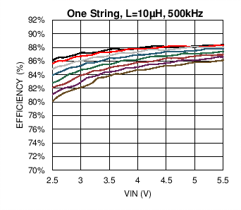
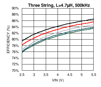
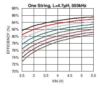
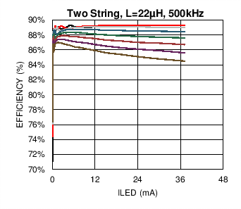
Application Performance Plots

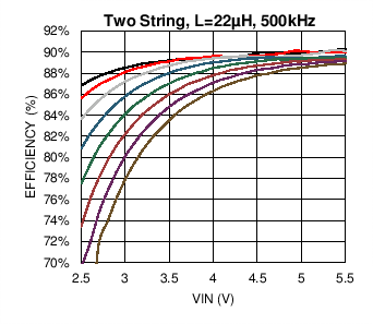
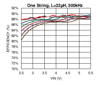
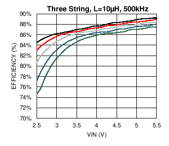
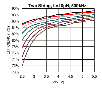
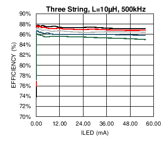
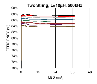
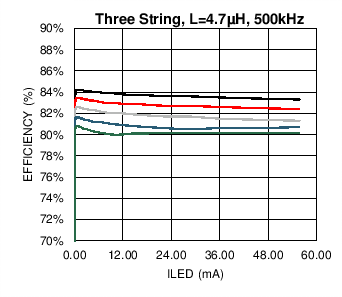
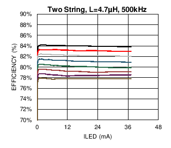
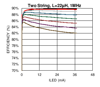
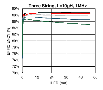
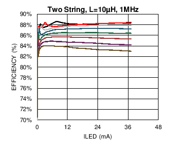
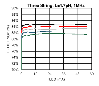
VIN = 3.6 V, full-scale current = 20.2 mA, LEDs are WLEDs part # SML-312WBCW(A), Typical Application Circuit , TA = 25°C unless otherwise specified. Efficiency is VOUT × (IHVLED1 + IHVLED2 + IHVLED3)/(VIN × IIN), matching curves are (ΔILED_MAX/ILED_AVE).
LM3697 C004_SNOSC2.png
Top to Bottom: 3x3, 3x4, 3x5, 3x6, 3x7 (LEDs)
Figure 16. Boost Efficiency vs VIN
LM3697 C007_SNOSC2.png
Top to Bottom: 3x3, 3x4, 3x5, 3x6, 3x7 (LEDs)
Figure 17. Boost Efficiency vs VIN
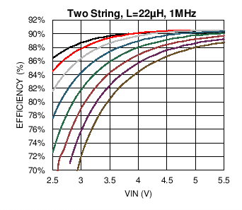
LM3697 C010_SNOSC2.png
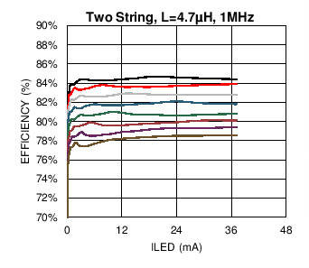
Top to Bottom: 2x3, 2x4, 2x5, 2x6, 2x7, 2x8, 2x9, 2x10 (LEDs)
Figure 18. Boost Efficiency vs VIN
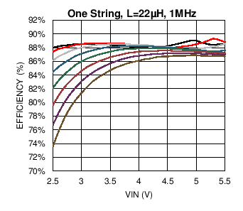
LM3697 C016_SNOSC2.png
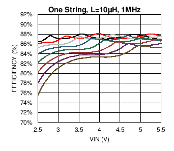
Top to Bottom: 1x3, 1x4, 1x5, 1x6, 1x7, 1x8, 1x9, 1x10 (LEDs)
Figure 20. Boost Efficiency vs VIN
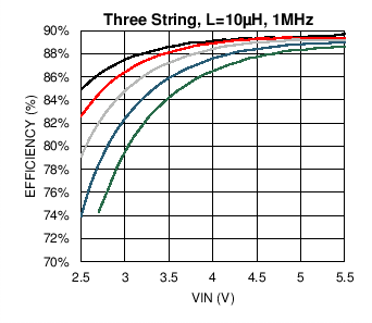
LM3697 C003_SNOSC2.png
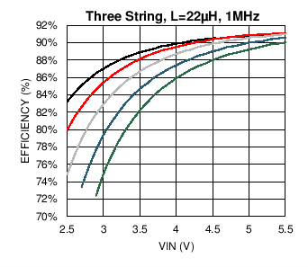
Top to Bottom: 3x3, 3x4, 3x5, 3x6, 3x7 (LEDs)
Figure 22. Boost Efficiency vs VIN
LM3697 C009_SNOSC2.png
Top to Bottom: 2x3, 2x4, 2x5, 2x6, 2x7, 2x8, 2x9, 2x10 (LEDs)
Figure 24. Boost Efficiency vs VIN
LM3697 C015_SNOSC2.png
Top to Bottom: 1x3, 1x4, 1x5, 1x6, 1x7, 1x8, 1x9, 1x10 (LEDs)
Figure 26. Boost Efficiency vs VIN
LM3697 C002_SNOSC2.png
Top to Bottom: 3x3, 3x4, 3x5, 3x6, 3x7 (LEDs)
Figure 28. Boost Efficiency vs VIN
LM3697 C008_SNOSC2.png
Top to Bottom: 2x3, 2x4, 2x5, 2x6, 2x7, 2x8, 2x9, 2x10 (LEDs)
Figure 30. Boost Efficiency vs VIN
LM3697 C014_SNOSC2.png
Top to Bottom: 1x3, 1x4, 1x5, 1x6, 1x7, 1x8, 1x9, 1x10 (LEDs)
Figure 32. Boost Efficiency vs VIN
LM3697 C022_SNOSC2.png
Top to Bottom: 3x3, 3x4, 3x5, 3x6, 3x7 (LEDs)
Figure 34. Boost Efficiency vs ILED
LM3697 C028_SNOSC2.png
Top to Bottom: 2x3, 2x4, 2x5, 2x6, 2x7, 2x8, 2x9, 2x10 (LEDs)
Figure 36. Boost Efficiency vs ILED
LM3697 C021_SNOSC2.png
Top to Bottom: 3x3, 3x4, 3x5, 3x6, 3x7 (LEDs)
Figure 38. Boost Efficiency vs ILED
LM3697 C027_SNOSC2.png
Top to Bottom: 2x3, 2x4, 2x5, 2x6, 2x7, 2x8, 2x9, 2x10 (LEDs)
Figure 40. Boost Efficiency vs ILED
LM3697 C020_SNOSC2.png
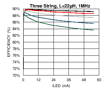
Top to Bottom: 3x3, 3x4, 3x5, 3x6, 3x7 (LEDs)
Figure 42. Boost Efficiency vs ILED
LM3697 C026_SNOSC2.png
Top to Bottom: 2x3, 2x4, 2x5, 2x6, 2x7, 2x8, 2x9, 2x10 (LEDs)
Figure 44. Boost Efficiency vs ILED
LM3697 C001_SNOSC2.png
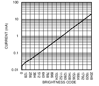
Exponential Mapping
Figure 46. HVLED Current vs. Brightness Code
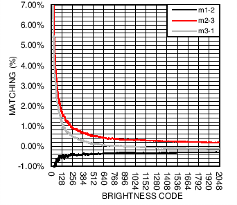
LM3697 C042_SNOSC2.png
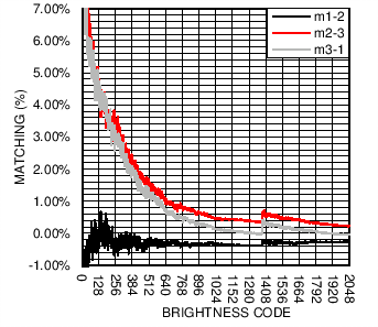
Linear Mapping
Figure 48. HVLED Matching Vs. Brightness Code
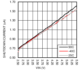
LM3697 C040_SNOSC2.png
Figure 50. Shutdown Current vs. VIN
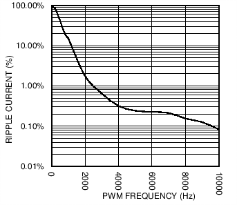
LM3697 C043_SNOSC2.pngFigure 52. Led Current Ripple vs FPWM
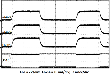
LM3697 pwm_step2.png
Figure 54. Response To Step Change In PWM Input Duty Cycle
LM3697 vin_step_scaled.png
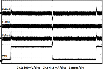
Figure 56. Line Step Response
LM3697 C013_SNOSC2.png
Top to Bottom: 2x3, 2x4, 2x5, 2x6, 2x7, 2x8, 2x9, 2x10 (LEDs)
Figure 19. Boost Efficiency vs VIN
LM3697 C019_SNOSC2.png
Top to Bottom: 1x3, 1x4, 1x5, 1x6, 1x7, 1x8, 1x9, 1x10 (LEDs)
Figure 21. Boost Efficiency vs VIN
LM3697 C006_SNOSC2.png
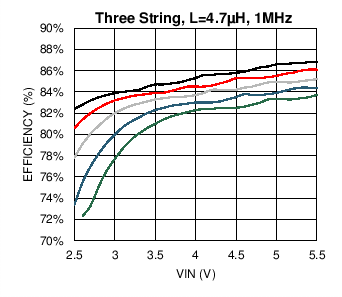
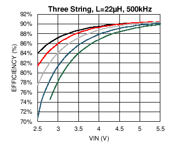
Top to Bottom: 3x3, 3x4, 3x5, 3x6, 3x7 (LEDs)
Figure 23. Boost Efficiency vs VIN
LM3697 C012_SNOSC2.png
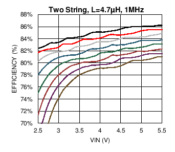
Top to Bottom: 2x3, 2x4, 2x5, 2x6, 2x7, 2x8, 2x9, 2x10 (LEDs)
Figure 25. Boost Efficiency V vs VIN
LM3697 C018_SNOSC2.png
Top to Bottom: 1x3, 1x4, 1x5, 1x6, 1x7, 1x8, 1x9, 1x10 (LEDs)
Figure 27. Boost Efficiency vs VIN
LM3697 C005_SNOSC2.png
Top to Bottom: 3x3, 3x4, 3x5, 3x6, 3x7 (LEDs)
Figure 29. Boost Efficiency vs VIN
LM3697 C011_SNOSC2.png
Top to Bottom: 2x3, 2x4, 2x5, 2x6, 2x7, 2x8, 2x9, 2x10 (LEDs)
Figure 31. Boost Efficiency vs VIN
LM3697 C017_SNOSC2.png
Top to Bottom: 1x3, 1x4, 1x5, 1x6, 1x7, 1x8, 1x9, 1x10 (LEDs)
Figure 33. Boost Efficiency vs VIN
LM3697 C025_SNOSC2.png
Top to Bottom: 3x3, 3x4, 3x5, 3x6, 3x7 (LEDs)
Figure 35. Boost Efficiency vs ILED
LM3697 C031_SNOSC2.png
Top to Bottom: 2x3, 2x4, 2x5, 2x6, 2x7, 2x8, 2x9, 2x10 (LEDs)
Figure 37. Boost Efficiency vs ILED
LM3697 C024_SNOSC2.png
Top to Bottom: 3x3, 3x4, 3x5, 3x6, 3x7 (LEDs)
Figure 39. Boost Efficiency vs ILED
LM3697 C030_SNOSC2.png
Top to Bottom: 2x3, 2x4, 2x5, 2x6, 2x7, 2x8, 2x9, 2x10 (LEDs)
Figure 41. Boost Efficiency vs ILED
LM3697 C023_SNOSC2.png
Top to Bottom: 3x3, 3x4, 3x5, 3x6, 3x7 (LEDs)
Figure 43. Boost Efficiency vs ILED
LM3697 C029_SNOSC2.png
Top to Bottom: 2x3, 2x4, 2x5, 2x6, 2x7, 2x8, 2x9, 2x10 (LEDs)
Figure 45. Boost Efficiency vs ILED
LM3697 C041_SNOSC2.png
Exponential Mapping
Figure 47. HVLED Matching Vs. Brightness Code
LM3697 C046_SNOSC2.png
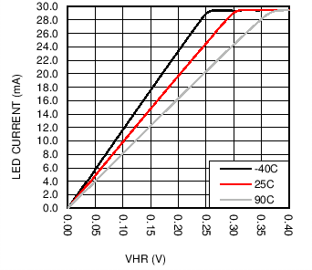
Figure 49. HVLED Current vs. Current Sink Headroom Voltage
LM3697 C045_SNOSC2.png
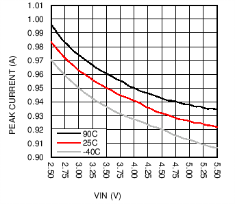
Figure 51. Open Loop Current Limit vs. VIN
LM3697 startup_exp.png
8s2p LED configuration
Figure 53. Start-up Response
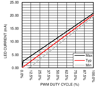
LM3697 C044_SNOSC2.pngFigure 55. HVLED Current Vs PWM Input Duty Cycle