SNOSCS2D November   2013  – March 2019 LM3697

PRODUCTION DATA.  

  1. Features
  2. Applications
  3. Description
    1.     Device Images
      1.      Simplified Schematic
      2.      Boost Efficiency
  4. Revision History
  5. Pin Configuration and Functions
    1.     Pin Functions
  6. Specifications
    1. 6.1 Absolute Maximum Ratings
    2. 6.2 ESD Ratings
    3. 6.3 Recommended Operating Conditions
    4. 6.4 Thermal Information
    5. 6.5 Electrical Characteristics
    6. 6.6 Timing Requirements
    7. 6.7 Typical Characteristics
  7. Detailed Description
    1. 7.1 Overview
      1. 7.1.1 PWM Input
      2. 7.1.2 HWEN Input
      3. 7.1.3 Thermal Shutdown
    2. 7.2 Functional Block Diagram
    3. 7.3 Feature Descriptions
      1. 7.3.1 High-Voltage LED Control
        1. 7.3.1.1 High-Voltage Boost Converter
        2. 7.3.1.2 High-Voltage Current Sinks (HVLED1, HVLED2 and HVLED3)
        3. 7.3.1.3 High-Voltage Current String Biasing
      2. 7.3.2 Boost Switching-Frequency Select
      3. 7.3.3 Automatic Switching Frequency Shift
      4. 7.3.4 Brightness Register Current Control
        1. 7.3.4.1 8-Bit Control (Preferred)
        2. 7.3.4.2 11-Bit Control
      5. 7.3.5 PWM Control
        1. 7.3.5.1 PWM Input Frequency Range
        2. 7.3.5.2 PWM Input Polarity
        3. 7.3.5.3 PWM Zero Detection
      6. 7.3.6 Start-up/Shutdown Ramp
      7. 7.3.7 Run-Time Ramp
      8. 7.3.8 High-Voltage Control A and B Ramp Select
    4. 7.4 Device Functional Modes
      1. 7.4.1 LED Current Mapping Modes
        1. 7.4.1.1 Exponential Mapping
          1. 7.4.1.1.1 8-Bit Code Calculation
          2. 7.4.1.1.2 11-Bit Code Calculation
        2. 7.4.1.2 Linear Mapping
          1. 7.4.1.2.1 8-Bit Code Calculation
          2. 7.4.1.2.2 11-Bit Code Calculation
      2. 7.4.2 Fault Flags/Protection Features
        1. 7.4.2.1 Open LED String (HVLED)
        2. 7.4.2.2 Shorted LED String (HVLED)
        3. 7.4.2.3 Overvoltage Protection (Inductive Boost)
        4. 7.4.2.4 Current Limit (Inductive Boost)
      3. 7.4.3 I2C-Compatible Interface
        1. 7.4.3.1 Start And Stop Conditions
        2. 7.4.3.2 I2C-Compatible Address
        3. 7.4.3.3 Transferring Data
        4. 7.4.3.4 High-Speed Mode
    5. 7.5 Register Maps
  8. Application and Implementation
    1. 8.1 Application Information
    2. 8.2 Typical Applications
      1. 8.2.1 Design Requirements
      2. 8.2.2 Detailed Design Procedure
        1. 8.2.2.1 Boost Converter Maximum Output Power
          1. 8.2.2.1.1 Peak Current Limited
          2. 8.2.2.1.2 Output Voltage Limited
        2. 8.2.2.2 Inductor Selection
        3. 8.2.2.3 Output Capacitor Selection
        4. 8.2.2.4 Schottky Diode Selection
        5. 8.2.2.5 Input Capacitor Selection
        6. 8.2.2.6 Application Circuit Component List
      3. 8.2.3 Application Performance Plots
    3. 8.3 Initialization Set Up
  9. Power Supply Recommendations
  10. 10Layout
    1. 10.1 Layout Guidelines
      1. 10.1.1 Boost Output Capacitor Placement
      2. 10.1.2 Schottky Diode Placement
      3. 10.1.3 Inductor Placement
      4. 10.1.4 Boost Input Capacitor Placement
    2. 10.2 Layout Example
  11. 11Device and Documentation Support
    1. 11.1 Device Support
      1. 11.1.1 Third-Party Products Disclaimer
    2. 11.2 Related Documentation
    3. 11.3 Receiving Notification of Documentation Updates
    4. 11.4 Community Resources
    5. 11.5 Trademarks
    6. 11.6 Electrostatic Discharge Caution
    7. 11.7 Glossary
  12. 12Mechanical, Packaging, and Orderable Information

Package Options

Refer to the PDF data sheet for device specific package drawings

Mechanical Data (Package|Pins)
  • YFQ|12
Thermal pad, mechanical data (Package|Pins)
Orderable Information

Pin Configuration and Functions

YFQ Package
12-Pin DSBGA
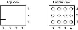
LM3697 Pkg_outline.gif

Pin Functions

PIN TYPE DESCRIPTION
NUMBER NAME
A1 PWM Input PWM brightness control input for CABC operation. PWM is a high-impedance input and cannot be left floating, if not used connect to GND.
A2 SDA I/O Serial data connection for I2C-compatible interface.
A3 HWEN Input Hardware enable input. Drive this pinl high to enable the device. Drive this pin low to force the device into a low power shutdown. HWEN is a high-impedance input and cannot be left floating.
B1 HVLED1 Input Input pin to high-voltage current sink 1 (40 V maximum). The boost converter regulates the minimum of HVLED1, HVLED2 and HVLED3 to VHR.
B2 SCL Input Serial clock connection for I2C-compatible interface.
B3 IN Input Input voltage connection. Bypass IN to GND with a minimum 2.2-µF ceramic capacitor.
C1 HVLED2 Input Input pin to high-voltage current sink 2 (40 V maximum). The boost converter regulates the minimum of HVLED1, HVLED2 and HVLED3 to VHR.
C2 GND GND Ground
C3 GND GND Ground
D1 HVLED3 Input Input pin to high-voltage current sink 3 (40 V maximum). The boost converter regulates the minimum of HVLED1, HVLED2 and HVLED3 to VHR.
D2 OVP Input Overvoltage sense input. Connect OVP to the positive terminal of the inductive boost's output capacitor (COUT).
D3 SW Output Drain connection for the internal NFET. Connect SW to the junction of the inductor and the Schottky diode anode.