SNOSCS2D November   2013  – March 2019 LM3697

PRODUCTION DATA.  

  1. Features
  2. Applications
  3. Description
    1.     Device Images
      1.      Simplified Schematic
      2.      Boost Efficiency
  4. Revision History
  5. Pin Configuration and Functions
    1.     Pin Functions
  6. Specifications
    1. 6.1 Absolute Maximum Ratings
    2. 6.2 ESD Ratings
    3. 6.3 Recommended Operating Conditions
    4. 6.4 Thermal Information
    5. 6.5 Electrical Characteristics
    6. 6.6 Timing Requirements
    7. 6.7 Typical Characteristics
  7. Detailed Description
    1. 7.1 Overview
      1. 7.1.1 PWM Input
      2. 7.1.2 HWEN Input
      3. 7.1.3 Thermal Shutdown
    2. 7.2 Functional Block Diagram
    3. 7.3 Feature Descriptions
      1. 7.3.1 High-Voltage LED Control
        1. 7.3.1.1 High-Voltage Boost Converter
        2. 7.3.1.2 High-Voltage Current Sinks (HVLED1, HVLED2 and HVLED3)
        3. 7.3.1.3 High-Voltage Current String Biasing
      2. 7.3.2 Boost Switching-Frequency Select
      3. 7.3.3 Automatic Switching Frequency Shift
      4. 7.3.4 Brightness Register Current Control
        1. 7.3.4.1 8-Bit Control (Preferred)
        2. 7.3.4.2 11-Bit Control
      5. 7.3.5 PWM Control
        1. 7.3.5.1 PWM Input Frequency Range
        2. 7.3.5.2 PWM Input Polarity
        3. 7.3.5.3 PWM Zero Detection
      6. 7.3.6 Start-up/Shutdown Ramp
      7. 7.3.7 Run-Time Ramp
      8. 7.3.8 High-Voltage Control A and B Ramp Select
    4. 7.4 Device Functional Modes
      1. 7.4.1 LED Current Mapping Modes
        1. 7.4.1.1 Exponential Mapping
          1. 7.4.1.1.1 8-Bit Code Calculation
          2. 7.4.1.1.2 11-Bit Code Calculation
        2. 7.4.1.2 Linear Mapping
          1. 7.4.1.2.1 8-Bit Code Calculation
          2. 7.4.1.2.2 11-Bit Code Calculation
      2. 7.4.2 Fault Flags/Protection Features
        1. 7.4.2.1 Open LED String (HVLED)
        2. 7.4.2.2 Shorted LED String (HVLED)
        3. 7.4.2.3 Overvoltage Protection (Inductive Boost)
        4. 7.4.2.4 Current Limit (Inductive Boost)
      3. 7.4.3 I2C-Compatible Interface
        1. 7.4.3.1 Start And Stop Conditions
        2. 7.4.3.2 I2C-Compatible Address
        3. 7.4.3.3 Transferring Data
        4. 7.4.3.4 High-Speed Mode
    5. 7.5 Register Maps
  8. Application and Implementation
    1. 8.1 Application Information
    2. 8.2 Typical Applications
      1. 8.2.1 Design Requirements
      2. 8.2.2 Detailed Design Procedure
        1. 8.2.2.1 Boost Converter Maximum Output Power
          1. 8.2.2.1.1 Peak Current Limited
          2. 8.2.2.1.2 Output Voltage Limited
        2. 8.2.2.2 Inductor Selection
        3. 8.2.2.3 Output Capacitor Selection
        4. 8.2.2.4 Schottky Diode Selection
        5. 8.2.2.5 Input Capacitor Selection
        6. 8.2.2.6 Application Circuit Component List
      3. 8.2.3 Application Performance Plots
    3. 8.3 Initialization Set Up
  9. Power Supply Recommendations
  10. 10Layout
    1. 10.1 Layout Guidelines
      1. 10.1.1 Boost Output Capacitor Placement
      2. 10.1.2 Schottky Diode Placement
      3. 10.1.3 Inductor Placement
      4. 10.1.4 Boost Input Capacitor Placement
    2. 10.2 Layout Example
  11. 11Device and Documentation Support
    1. 11.1 Device Support
      1. 11.1.1 Third-Party Products Disclaimer
    2. 11.2 Related Documentation
    3. 11.3 Receiving Notification of Documentation Updates
    4. 11.4 Community Resources
    5. 11.5 Trademarks
    6. 11.6 Electrostatic Discharge Caution
    7. 11.7 Glossary
  12. 12Mechanical, Packaging, and Orderable Information

Package Options

Refer to the PDF data sheet for device specific package drawings

Mechanical Data (Package|Pins)
  • YFQ|12
Thermal pad, mechanical data (Package|Pins)
Orderable Information

PWM Control

The LM3697's PWM input can be enabled for Control Banks A or B (see Table 14). Once enabled, the LED current becomes a function of the code in the Control Bank Brightness Configuration Register and the PWM input-duty cycle.

The PWM input accepts a logic level voltage and internally filters it to an analog control voltage. This results in a linear response of duty cycle to current, where 100% duty cycle corresponds to the programmed brightness code multiplied by the Full-Scale Current setting.
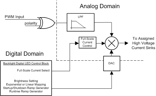
LM3697 pwm_arch.gifFigure 9. PWM Input Architecture