SNOSCS2D November   2013  – March 2019 LM3697

PRODUCTION DATA.  

  1. Features
  2. Applications
  3. Description
    1.     Device Images
      1.      Simplified Schematic
      2.      Boost Efficiency
  4. Revision History
  5. Pin Configuration and Functions
    1.     Pin Functions
  6. Specifications
    1. 6.1 Absolute Maximum Ratings
    2. 6.2 ESD Ratings
    3. 6.3 Recommended Operating Conditions
    4. 6.4 Thermal Information
    5. 6.5 Electrical Characteristics
    6. 6.6 Timing Requirements
    7. 6.7 Typical Characteristics
  7. Detailed Description
    1. 7.1 Overview
      1. 7.1.1 PWM Input
      2. 7.1.2 HWEN Input
      3. 7.1.3 Thermal Shutdown
    2. 7.2 Functional Block Diagram
    3. 7.3 Feature Descriptions
      1. 7.3.1 High-Voltage LED Control
        1. 7.3.1.1 High-Voltage Boost Converter
        2. 7.3.1.2 High-Voltage Current Sinks (HVLED1, HVLED2 and HVLED3)
        3. 7.3.1.3 High-Voltage Current String Biasing
      2. 7.3.2 Boost Switching-Frequency Select
      3. 7.3.3 Automatic Switching Frequency Shift
      4. 7.3.4 Brightness Register Current Control
        1. 7.3.4.1 8-Bit Control (Preferred)
        2. 7.3.4.2 11-Bit Control
      5. 7.3.5 PWM Control
        1. 7.3.5.1 PWM Input Frequency Range
        2. 7.3.5.2 PWM Input Polarity
        3. 7.3.5.3 PWM Zero Detection
      6. 7.3.6 Start-up/Shutdown Ramp
      7. 7.3.7 Run-Time Ramp
      8. 7.3.8 High-Voltage Control A and B Ramp Select
    4. 7.4 Device Functional Modes
      1. 7.4.1 LED Current Mapping Modes
        1. 7.4.1.1 Exponential Mapping
          1. 7.4.1.1.1 8-Bit Code Calculation
          2. 7.4.1.1.2 11-Bit Code Calculation
        2. 7.4.1.2 Linear Mapping
          1. 7.4.1.2.1 8-Bit Code Calculation
          2. 7.4.1.2.2 11-Bit Code Calculation
      2. 7.4.2 Fault Flags/Protection Features
        1. 7.4.2.1 Open LED String (HVLED)
        2. 7.4.2.2 Shorted LED String (HVLED)
        3. 7.4.2.3 Overvoltage Protection (Inductive Boost)
        4. 7.4.2.4 Current Limit (Inductive Boost)
      3. 7.4.3 I2C-Compatible Interface
        1. 7.4.3.1 Start And Stop Conditions
        2. 7.4.3.2 I2C-Compatible Address
        3. 7.4.3.3 Transferring Data
        4. 7.4.3.4 High-Speed Mode
    5. 7.5 Register Maps
  8. Application and Implementation
    1. 8.1 Application Information
    2. 8.2 Typical Applications
      1. 8.2.1 Design Requirements
      2. 8.2.2 Detailed Design Procedure
        1. 8.2.2.1 Boost Converter Maximum Output Power
          1. 8.2.2.1.1 Peak Current Limited
          2. 8.2.2.1.2 Output Voltage Limited
        2. 8.2.2.2 Inductor Selection
        3. 8.2.2.3 Output Capacitor Selection
        4. 8.2.2.4 Schottky Diode Selection
        5. 8.2.2.5 Input Capacitor Selection
        6. 8.2.2.6 Application Circuit Component List
      3. 8.2.3 Application Performance Plots
    3. 8.3 Initialization Set Up
  9. Power Supply Recommendations
  10. 10Layout
    1. 10.1 Layout Guidelines
      1. 10.1.1 Boost Output Capacitor Placement
      2. 10.1.2 Schottky Diode Placement
      3. 10.1.3 Inductor Placement
      4. 10.1.4 Boost Input Capacitor Placement
    2. 10.2 Layout Example
  11. 11Device and Documentation Support
    1. 11.1 Device Support
      1. 11.1.1 Third-Party Products Disclaimer
    2. 11.2 Related Documentation
    3. 11.3 Receiving Notification of Documentation Updates
    4. 11.4 Community Resources
    5. 11.5 Trademarks
    6. 11.6 Electrostatic Discharge Caution
    7. 11.7 Glossary
  12. 12Mechanical, Packaging, and Orderable Information

Package Options

Refer to the PDF data sheet for device specific package drawings

Mechanical Data (Package|Pins)
  • YFQ|12
Thermal pad, mechanical data (Package|Pins)
Orderable Information

Peak Current Limited

In the case of a peak current limited situation, when the peak of the inductor current hits the LM3697 device's current limit, the NFET switch turns off for the remainder of the switching period. If this happens each switching cycle the LM3697 regulates the peak of the inductor current instead of the headroom across the current sinks. This can result in the dropout of the boost output connected current sinks, and the LED current dropping below its programmed level.

The peak current in a boost converter is dependent on the value of the inductor, total LED current in the boost (IOUT), the boost output voltage (VOUT) (which is the highest voltage LED string + VHR ), the input voltage (VIN), the switching frequency (ƒSW), and the efficiency (output power/input power). Additionally, the peak current is different depending on whether the inductor current is continuous during the entire switching period (CCM), or discontinuous (DCM) where it goes to 0 before the switching period ends. For CCM the peak inductor current is given by:

Equation 9. LM3697 eq02-new.gif

For DCM the peak inductor current is given by:

Equation 10. LM3697 eq3.gif

To determine which mode the circuit is operating in (CCM or DCM) it is necessary to perform a calculation to test whether the inductor current ripple is less than the anticipated input current (IIN). If ΔIL is less than IIN then the device is operating in CCM. If ΔIL is greater than IIN then the device is operating in DCM.

Equation 11. LM3697 eq04-new.gif

Typically at currents high enough to reach the LM3697's peak current limit, the device is operating in CCM.

Figure 14 and Figure 15 show the output current and voltage derating for a 10-µH and a 22-µH inductor. These plots take Equation 9 and Equation 10 and plot VOUT and IOUT with varying VIN, a constant peak current of 880 mA (ICL_MIN), 500-kHz switching frequency, and a constant efficiency of 85%. Using these curves can give a good design guideline on selecting the correct inductor for a given output power requirement. A 10-µH inductor will typically be a smaller device with lower on resistance, but the peak currents is higher. A 22-µH inductor provides for lower peak currents but a larger sized device is required to match the DC resistance of a 10-µH inductor.
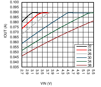
LM3697 C052_SNOSC2.pngFigure 14. Maximum Output Power (22 µH)
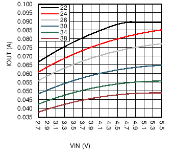
LM3697 C051_SNOSC2.pngFigure 15. Maximum Output Power (10 µH)