SNVS533D September 2007 – November 2014 LM4510
PRODUCTION DATA.
- 1 Features
- 2 Applications
- 3 Description
- 4 Revision History
- 5 Pin Configuration and Functions
- 6 Specifications
- 7 Detailed Description
-
8 Application and Implementation
- 8.1 Application Information
- 8.2
Typical Applications
- 8.2.1
2.7 V to 5.5 V Input with a 16 V Output
- 8.2.1.1 Design Requirements
- 8.2.1.2
Detailed Design Procedure
- 8.2.1.2.1 Adjusting Output Voltage
- 8.2.1.2.2 Maximum Output Current
- 8.2.1.2.3 Inductor Selection
- 8.2.1.2.4 IL_AVE Check
- 8.2.1.2.5 Input Capacitor Selection
- 8.2.1.2.6 Output Capacitor Selection
- 8.2.1.2.7 Soft-Start Function and Soft-Start Capacitor Selection
- 8.2.1.2.8 Compensation Component Selection
- 8.2.1.3 Application Curves
- 8.2.2 Flash and Torch Application
- 8.2.1
2.7 V to 5.5 V Input with a 16 V Output
- 9 Power Supply Recommendations
- 10Layout
- 11Device and Documentation Support
- 12Mechanical, Packaging, and Orderable Information
Package Options
Mechanical Data (Package|Pins)
- DSC|10
Thermal pad, mechanical data (Package|Pins)
- DSC|10
Orderable Information
8 Application and Implementation
NOTE
Information in the following applications sections is not part of the TI component specification, and TI does not warrant its accuracy or completeness. TI’s customers are responsible for determining suitability of components for their purposes. Customers should validate and test their design implementation to confirm system functionality.
8.1 Application Information
The LM4510 shuts down when the EN pin is low. In this mode the feedback resistors and the load are disconnected from the input in order to avoid leakage current flow and to allow the output voltage to drop to 0 V.
The LM4510 turns on when EN is high. There is an internal pull-down resistor on the EN pin so the device is in a normally off state.
8.2 Typical Applications
8.2.1 2.7 V to 5.5 V Input with a 16 V Output
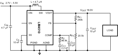 Figure 18. Typical Application Circuit for Normal DC/DC
8.2.1.1 Design Requirements
The LM4510 is designed to operate up to 75 mA at 2.7 V input and 350 mA at 5.5 V input to output 16 V. In any case, it is recommended to avoid starting up the device at minimum input voltage and maximum load. Special attention must be taken to avoid operating near thermal shutdown condition. A simple calculation can be used to determine the power dissipation at the operating condition. PD-MAX = (TJ-MAX-OP – TA-MAX)/RθJA(TJ-MAX-OP = 125°C).
8.2.1.2 Detailed Design Procedure
8.2.1.2.1 Adjusting Output Voltage
The output voltage is set using the feedback pin and a resistor voltage divider (RF1, RF2) connected to the output as shown in Figure 18.
The ratio of the feedback resistors sets the output voltage.
-
RF2 Selection
First of all choose a value for RF2 generally between 10 kΩ and 25 kΩ.
-
RF1 Selection
Calculate RF1 using Equation 1:
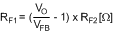
Table 1 gives suggested component values for several typical output voltages.
Table 1. Suggested Component Values for Different Output Voltages
| OUTPUT VOLTAGE (V) | RF2 (kΩ) | RF1 (kΩ) | RC (kΩ) | CC1 (nF) |
|---|---|---|---|---|
| 16 | 20.5 | 240 | 46.4 | 2.2 |
| 12 | 20.5 | 174 | 46.4 | 2.2 |
| 5 | 20.5 | 60.4 | 46.4 | 2.2 |
| 3.3 | 20.5 | 33 | 46.4 | 2.2 |
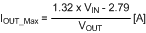
8.2.1.2.2 Maximum Output Current
When the output voltage is set at different level, it is important to know the maximum load capability. By first order estimation, IOUT(MAX) can be estimated by Equation 2:
8.2.1.2.3 Inductor Selection
The larger value inductor makes lower peak inductor current and reduces stress on internal power NMOS.
On the other hand, the smaller value inductor has smaller outline, lower DCR and a higher current capacity. Generally a 4.7-μH to 15-μH inductor is recommended.
8.2.1.2.4 IL_AVE Check
The average inductor current is given by Equation 3:
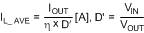
Where IOUT is output current, η is the converter efficiency of the total driven load and D’ is the off duty cycle of the switching regulator.
Inductor DC current rating (40°C temperature rise) should be more than the average inductor current at worst case.
ΔI Define
The inductor ripple current is given by Equation 4:
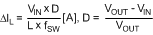
Where D is the on-duty cycle of the switching regulator. A common choice is to set ΔIL to about 30% of IL_AVE.
IL_PK≤ ICL Check & IMIN Define
The peak inductor current is given by Equation 5:
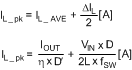
To prevent loss of regulation, ensure that the NMOS power switch current limit is greater than the worst-case peak inductor current in the target application.
Also make sure that the inductor saturation current is greater than the peak inductor current under the worst-case load transient, high ambient temperature and start-up conditions. Refer to Table 2 for suggested inductors.
Table 2. Suggested Inductors and Their Suppliers
| MODEL | VENDOR | DIMENSIONS LxWxH (mm) | D.C.R (max) |
|---|---|---|---|
| DO3314-472ML | COILCRAFT | 3.3mm x 3.3mm x 1.4mm | 320 mΩ |
| DO3316P-472ML | COILCRAFT | 12.95mm x 9.4mm x 5.4mm | 18 mΩ |
8.2.1.2.5 Input Capacitor Selection
Due to the presence of an inductor, the input current waveform is continuous and triangular. So the input capacitor is less critical than output capacitor in boost applications. Typically, a 4.7-μF to 10-μF ceramic input capacitor is recommended on the VIN pin of the IC.
ICIN_RMS Check
The RMS current in the input capacitor is given by Equation 6:

The input capacitor should be capable of handling the RMS current.
8.2.1.2.6 Output Capacitor Selection
The output capacitor in a boost converter provides all the output current when the switch is closed and the inductor is charging. As a result, it sees very large ripple currents.
A ceramic capacitor of value 4.7 μF to 10 μF is recommended at the output. If larger amounts of capacitance are desired for improved line support and transient response, tantalum capacitors can be used.
ICOUT_RMS Check
The RMS current in the output capacitor is given by Equation 7:
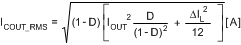
The output capacitor should be capable of handling the RMS current.
The ESR and ESL of the output capacitor directly control the output ripple. Use capacitors with low ESR and ESL at the output for high efficiency and low ripple voltage. The output capacitor also affects the soft-start time (See Soft-Start Function and Soft-Start Capacitor Selection). Table 3 shows suggested input and output capacitors.
Table 3. Suggested CIN and COUT Capacitors and Their Suppliers
| MODEL | TYPE | VENDOR | VOLTAGE RATING | CASE SIZE INCH (mm) |
|---|---|---|---|---|
| 4.7 µF for CIN | ||||
| C2012X5R0J475 | Ceramic, X5R | TDK | 6.3 V | 0805 (2012) |
| GRM21BR60J475 | Ceramic, X5R | muRata | 6.3 V | 0805 (2012) |
| JMK212BJ475 | Ceramic, X5R | Taiyo-Yuden | 6.3 V | 0805 (2012) |
| C2012X5R0J475K | Ceramic, X5R | TDK | 6.3 V | 0603 (1608) |
| 10 µF for COUT | ||||
| TMK316BJ106KL | Ceramic, X5R | Taiyo-Yuden | 25 V | 1206 (3216) |
| 12103D106KAT2A | Ceramic, X5R | AVX | 25 V | 1210 (3225) |
8.2.1.2.7 Soft-Start Function and Soft-Start Capacitor Selection
The LM4510 has a soft-start pin that can be used to limit the input inrush current. Connect a capacitor from SS pin to GND to set the soft-start period. Figure 19 describes the soft start process.
- Initial charging period: When the device is turned on, the control circuitry linearly regulating initial charge current charges VOUT by limiting the inrush current.
- Soft-start period: After VOUT reaches VIN –0.7 V (typ.), the device starts switching and the CS is charged at a constant current of 11 μA, ramping up to VIN. This period ends when VSS reaches VFB. CS should be large enough to ensure soft-start period ends after CO is fully charged.
During the initial charging period, the required load current must be smaller than the initial charge current to ensure VOUT reaches VIN –0.7 V (typ.).
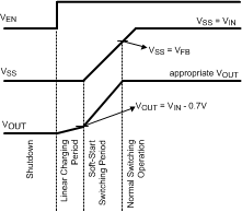 Figure 19. Soft-Start Timing Diagram
CS Selection
The soft-start time without load can be estimated as:
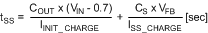
Where the IINIT_CHARGE is Initial Charging Current depending on VIN and ISS_CHARGE (11 μA (typ.). Also, when selecting the fuse current rating, make sure the value is higher than the initial charging current.
8.2.1.2.8 Compensation Component Selection
The LM4510 provides a compensation pin COMP to customize the voltage loop feedback. It is recommended that a series combination of RC and CC1 be used for the compensation network, as shown in the typical application circuit. In addition, CC2 is used for compensating high frequency zeros.
The series combination of RC and CC1 introduces a pole-zero pair according to Equation 9:
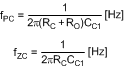
In addition, CC2 introduces a pole according to Equation 10:
Where RO is the output impedance of the error amplifier, approximately 1 MΩ, and amplifier voltage gain is typically 200 V/V depending on temperature and VIN.
Refer to Table 4 for suggested soft start capacitor and compensation components.
Table 4. Suggested CS and Compensation Components
| MODEL | TYPE | VENDOR | VOLTAGE RATING | CASE SIZE INCH (mm) |
|---|---|---|---|---|
| (CS) C1608C0G1E103J | Ceramic, X5R | TDK | 6.3 V | 603 (1608) |
| (C1)TMK107SD222JA-T | Ceramic, X5R | Taiyo Yuden | 25 V | 603 (1608) |
| (RC) 9t06031A4642FBHFT | Resistor | Yageo Corporation | 1/10 W | 603 (1608) |
8.2.1.3 Application Curves
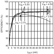 Figure 20. Efficiency vs Output Current (VOUT = 16 V)
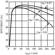
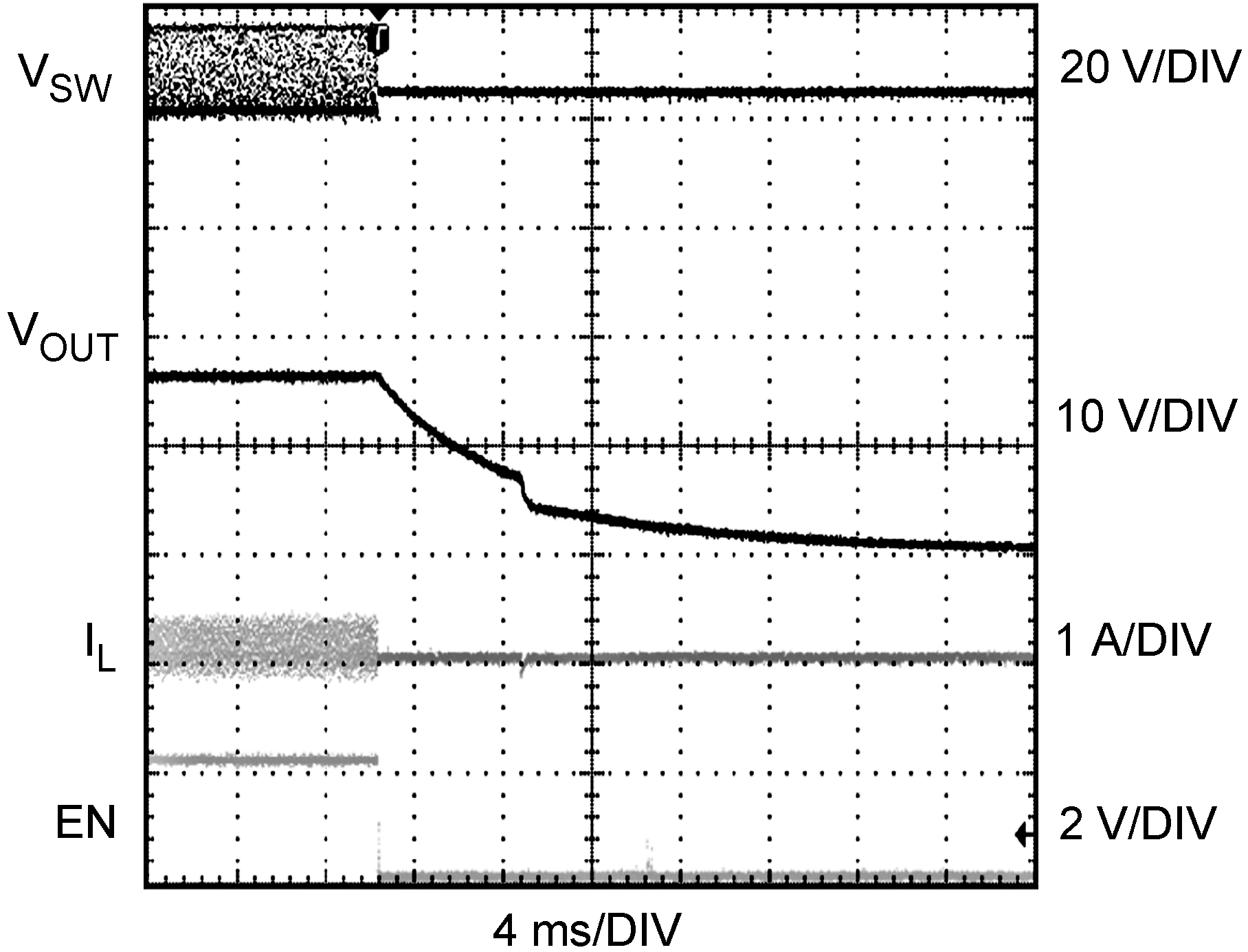 Figure 24. Shut Down (VOUT = 16 V, RLOAD = 940 Ω)
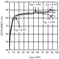 Figure 21. Efficiency vs Output Current (VOUT = 12 V)
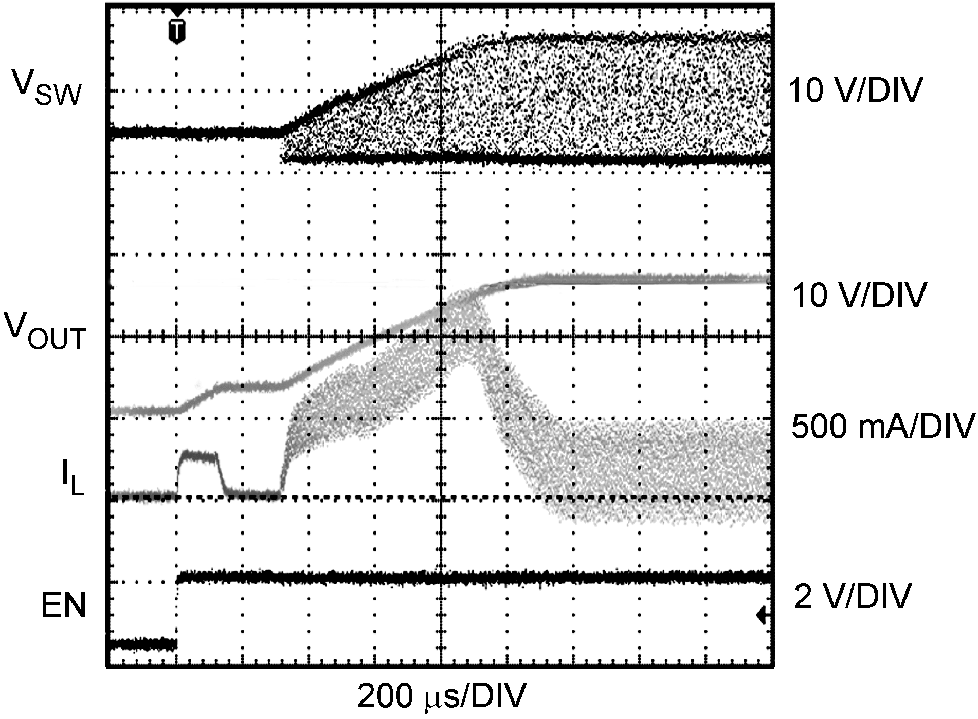 Figure 23. Start Up (VOUT = 16 V, RLOAD = 530 Ω)
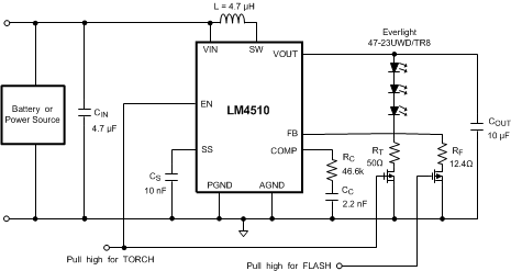
8.2.2 Flash and Torch Application
LM4510 can be configured to drive white LEDs for the flash and torch functions. The flash/torch can be set up with the circuit shown in Figure 25 by using the resistor RT to determine the current in Torch Mode and RF to determine the current in Flash Mode. The amount of current can be estimated using Equation 11:

8.2.2.1 Design Requirements
See Design Requirements.
8.2.2.2 Detailed Design Procedure
8.2.2.3 Application Curve
See Application Curves.