SNVS533D September 2007 – November 2014 LM4510
PRODUCTION DATA.
- 1 Features
- 2 Applications
- 3 Description
- 4 Revision History
- 5 Pin Configuration and Functions
- 6 Specifications
- 7 Detailed Description
-
8 Application and Implementation
- 8.1 Application Information
- 8.2
Typical Applications
- 8.2.1
2.7 V to 5.5 V Input with a 16 V Output
- 8.2.1.1 Design Requirements
- 8.2.1.2
Detailed Design Procedure
- 8.2.1.2.1 Adjusting Output Voltage
- 8.2.1.2.2 Maximum Output Current
- 8.2.1.2.3 Inductor Selection
- 8.2.1.2.4 IL_AVE Check
- 8.2.1.2.5 Input Capacitor Selection
- 8.2.1.2.6 Output Capacitor Selection
- 8.2.1.2.7 Soft-Start Function and Soft-Start Capacitor Selection
- 8.2.1.2.8 Compensation Component Selection
- 8.2.1.3 Application Curves
- 8.2.2 Flash and Torch Application
- 8.2.1
2.7 V to 5.5 V Input with a 16 V Output
- 9 Power Supply Recommendations
- 10Layout
- 11Device and Documentation Support
- 12Mechanical, Packaging, and Orderable Information
Package Options
Mechanical Data (Package|Pins)
- DSC|10
Thermal pad, mechanical data (Package|Pins)
- DSC|10
Orderable Information
7 Detailed Description
7.1 Overview
LM4510 is a peak current-mode, fixed-frequency PWM boost regulator that employs both Synchronous and Non-Synchronous Switching.
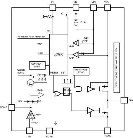
The DC/DC regulator regulates the feedback output voltage providing excellent line and load transient response. The operation of the LM4510 can best be understood by referring to the Block Diagram.
7.2 Functional Block Diagram
7.3 Feature Description
7.3.1 Short Circuit Protection
When VOUT goes down to VIN–0.7V (typ.), the device stops switching due to the short-circuit protection circuitry and the short-circuit output current is limited to IINIT_CHARGE.
7.3.2 Feedback Fault Protection
The LM4510 features unique Feedback Fault Protection to maximize safety when the feedback resistor is not properly connected to a circuit or the feedback node is shorted directly to ground.
Feedback fault triggers VOUT monitoring. During monitoring, if VOUT reaches a protection level, the device shuts down. When the feedback network is reconnected and VOUT is lower than the OFF threshold level of Feedback Fault Protection, VOUT monitoring stops. VOUT is then regulated by the control loop.
7.3.3 Input Undervoltage Lock-Out
The LM4510 has dedicated circuitry to protect the IC and the external components when the battery voltage is lower than the preset threshold. This undervoltage lock-out with hysteresis prevents malfunctions during start-up or abnormal power off.
7.3.4 Thermal Shutdown
If the die temperature exceeds 150°C (typ.), the thermal protection circuitry shuts down the device. The switches remain off until the die temperature is reduced to approximately 140°C (typ.).
7.4 Device Functional Modes
7.4.1 Non-Synchronous Operation
The device operates in Non-synchronous Mode at light load (IOUT < 10 mA) or when output voltage is lower than 10 V (typ.). At light load, LM4510 automatically changes its switching operation from 'Synchronous' to 'Non-Synchronous' depending on VIN and L. Non-Synchronous operation at light load maximizes power efficiency by reducing PMOS driving loss.
7.4.2 Operation in Synchronous Continuous Conduction Mode (Cycle 1, Cycle 2)
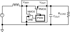 Figure 15. Schematic of Synchronous Boost Converter
Synchronous boost converter is shown in Figure 15. At the start of each cycle, the oscillator sets the driver logic and turns on the NMOS power device and turns off the PMOS power device.
7.4.2.1 Cycle 1 Description
Refer to Figure 16. NMOS switch turn-on → Inductor current increases and flows to GND.
PMOS switch turn-off → Isolate VOUT from SW → Output capacitor supplies load current.
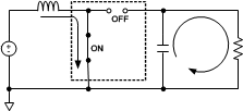 Figure 16. Equivalent Circuit During Cycle 1
During operation, EAMP output voltage (VCOMP) increases for larger loads and decreases for smaller loads. When the sum of the ramp compensation and the sensed NMOS current reaches a level determined by the EAMP output voltage, the PWM COMP resets the logic, turning off the NMOS power device and turning on the PMOS power device.
7.4.2.2 Cycle 2 Description
Refer to Figure 17. NMOS Switch turn-off → PMOS Switch turn-on→ Inductor current decreases and flows through PMOS → Inductor current recharges output capacitor and supplies load current.
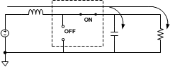 Figure 17. Equivalent Circuit During Cycle 2
After the switching period the oscillator then sets the driver logic again repeating the process.