SNVS533D September 2007 – November 2014 LM4510
PRODUCTION DATA.
- 1 Features
- 2 Applications
- 3 Description
- 4 Revision History
- 5 Pin Configuration and Functions
- 6 Specifications
- 7 Detailed Description
-
8 Application and Implementation
- 8.1 Application Information
- 8.2
Typical Applications
- 8.2.1
2.7 V to 5.5 V Input with a 16 V Output
- 8.2.1.1 Design Requirements
- 8.2.1.2
Detailed Design Procedure
- 8.2.1.2.1 Adjusting Output Voltage
- 8.2.1.2.2 Maximum Output Current
- 8.2.1.2.3 Inductor Selection
- 8.2.1.2.4 IL_AVE Check
- 8.2.1.2.5 Input Capacitor Selection
- 8.2.1.2.6 Output Capacitor Selection
- 8.2.1.2.7 Soft-Start Function and Soft-Start Capacitor Selection
- 8.2.1.2.8 Compensation Component Selection
- 8.2.1.3 Application Curves
- 8.2.2 Flash and Torch Application
- 8.2.1
2.7 V to 5.5 V Input with a 16 V Output
- 9 Power Supply Recommendations
- 10Layout
- 11Device and Documentation Support
- 12Mechanical, Packaging, and Orderable Information
Package Options
Mechanical Data (Package|Pins)
- DSC|10
Thermal pad, mechanical data (Package|Pins)
- DSC|10
Orderable Information
10 Layout
10.1 Layout Guidelines
High frequency switching regulators require very careful layout of components in order to get stable operation and low noise. All components must be as close as possible to the LM4510 device. Refer to Figure 26 as an example. Some additional guidelines to be observed:
- CIN must be placed close to the device and connected directly from VIN to PGND pins. This reduces copper trace resistance, which affects the input voltage ripple of the device. For additional input voltage filtering, typically a 0.1 uF bypass capacitor can be placed between VIN and AGND. This bypass capacitor should be placed near the device closer than CIN.
- COUT must also be placed close to the device and connected directly from VOUT to PGND pins. Any copper trace connections for the COUT capacitor can increase the series resistance, which directly affects output voltage ripple and makes noise during output voltage sensing.
- All voltage-sensing resistors (RF1, RF2) should be kept close to the FB pin to minimize copper trace connections that can inject noise into the system. The ground connection for the voltage-sensing resistor should be connected directly to the AGND pin.
- Trace connections made to the inductor should be minimized to reduce power dissipation, EMI radiation and increase overall efficiency. Also poor trace connection increases the ripple of SW.
- CS, CC1, CC2, RC must be placed close to the device and connected to AGND.
- The AGND pin should connect directly to the ground. Not connecting the AGND pin directly, as close to the chip as possible, may affect the performance of the LM4510 and limit its current driving capability. AGND and PGND should be separate planes and should be connected at a single point.
- For better thermal performance, DAP should be connected to ground, but cannot be used as the primary ground connection. The PC board land may be modified to a "dog bone" shape to reduce SON thermal impedance. For detail information, refer to Application Note AN-1187.
10.2 Layout Example
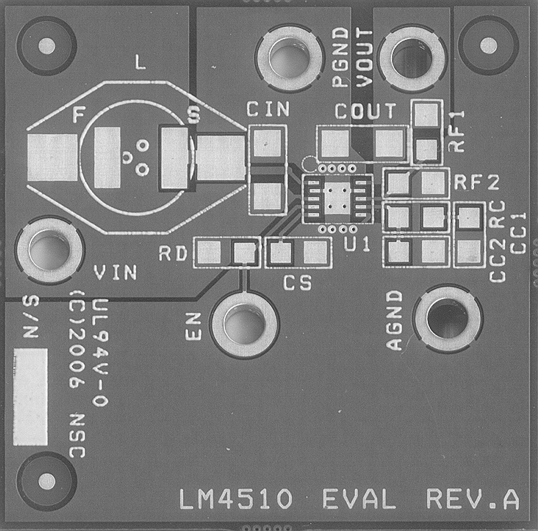 Figure 26. Evaluation Board Layout