SNVS496F January 2007 – May 2021 LM5002
PRODUCTION DATA
- 1 Features
- 2 Applications
- 3 Description
- 4 Revision History
- 5 Pin Configuration and Functions
- 6 Specifications
- 7 Detailed Description
- 8 Application and Implementation
- 9 Power Supply Recommendations
- 10Layout
- 11Device and Documentation Support
- 12Mechanical, Packaging, and Orderable Information
Package Options
Mechanical Data (Package|Pins)
Thermal pad, mechanical data (Package|Pins)
Orderable Information
8.2.1.2.6 Power Stage Analysis
In any switch-mode topology that has the power MOSFET between the inductor and the output capacitor (boost, buck-boost, Flyback, SEPIC, and so on) a Right Half-Plane Zero (RHPZ) is produced by the power stage in the loop transfer function during Continuous Conduction Mode (CCM). If the topology is operated in Discontinuous Conduction Mode (DCM), the RHPZ does not exist. It is a function of the duty cycle, load and inductance, and causes an increase in loop gain while reducing the loop phase margin. A common practice is to determine the worst case RHPZ frequency and set the loop unity gain frequency below one-third of the RHPZ frequency
In the Flyback topology, the equation for the RHPZ is given by Equation 14.
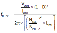
The worst case RHPZ frequency is at the maximum load where IOUT is the highest and at minimum input voltage where the duty cycle D is the highest. Assuming these conditions fRHPZ is 24.6 kHz.
The LM5002 uses slope compensation to ensure stability when the duty cycle exceeds 45%. This has the affect of adding some Voltage Mode control to this current-mode IC. The effect on the power stage (Plant) transfer function is calculated in the following equations:
Inductor current slope during MOSFET ON time (Equation 15)

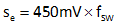
Slope compensation ramp (Equation 16)
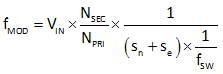
Current-mode sampling gain (Equation 17)
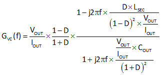
The control-to-output transfer function (GVC) using low ESR ceramic capacitors is Equation 18.
where:
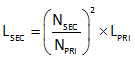
- LSEC is the transformer inductance referenced to the secondary side and is equal to:
Equation 19.
If high ESR capacitors (for example, aluminum electrolytic) are used for the output capacitance, an additional zero appears at frequency in Equation 20, which increases the gain slope by +20 dB per decade of frequency and boosts the phase 45° at FZERO(ESR) and 90° at 10 × FZERO(ESR).
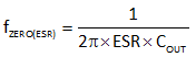
where:
- ESR is the series resistance of the output capacitor
- COUT is the output capacitance
With these calculations, an approximate power stage Bode plot can be constructed with Equation 21.
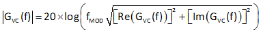
where:
- [Re(GVC(f))] is the real portion of
- [Im(GVC(f))] is the imaginary portion of
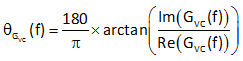
Because these equations don’t take into account the various parasitic resistances and reactances present in all power converters, there is some difference between the calculated Bode plot and the gain and phase of the actual circuit. It is therefore important to measure the converter using a network analyzer to quantify the implementation and adjust where appropriate.