SNVS496F January   2007  – May 2021 LM5002

PRODUCTION DATA  

  1. Features
  2. Applications
  3. Description
  4. Revision History
  5. Pin Configuration and Functions
  6. Specifications
    1. 6.1 Absolute Maximum Ratings
    2. 6.2 ESD Ratings
    3. 6.3 Recommended Operating Conditions
    4. 6.4 Thermal Information
    5. 6.5 Electrical Characteristics
    6. 6.6 Typical Characteristics
  7. Detailed Description
    1. 7.1 Overview
    2. 7.2 Functional Block Diagram
    3. 7.3 Feature Description
      1. 7.3.1 High Voltage VCC Regulator
      2. 7.3.2 Oscillator
      3. 7.3.3 External Synchronization
      4. 7.3.4 Enable and Standby
      5. 7.3.5 Error Amplifier and PWM Comparator
      6. 7.3.6 Current Amplifier and Slope Compensation
      7. 7.3.7 Power MOSFET
    4. 7.4 Device Functional Modes
      1. 7.4.1 Thermal Protection
  8. Application and Implementation
    1. 8.1 Application Information
      1. 8.1.1 VIN
      2. 8.1.2 SW PIN
      3. 8.1.3 EN or UVLO Voltage Divider Selection
      4. 8.1.4 Soft Start
    2. 8.2 Typical Applications
      1. 8.2.1 Non-Isolated Flyback Regulator
        1. 8.2.1.1 Design Requirements
        2. 8.2.1.2 Detailed Design Procedure
          1. 8.2.1.2.1 Switching Frequency
          2. 8.2.1.2.2 Flyback Transformer
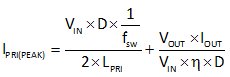
          3. 8.2.1.2.3 Peak MOSFET Current
          4. 8.2.1.2.4 Output Capacitance
          5. 8.2.1.2.5 Output Diode Rating
          6. 8.2.1.2.6 Power Stage Analysis
          7. 8.2.1.2.7 Loop Compensation
      2. 8.2.2 Isolated Flyback Regulator
        1. 8.2.2.1 Design Requirements
      3. 8.2.3 Boost Regulator
        1. 8.2.3.1 Design Requirements
      4. 8.2.4 24-V SEPIC Regulator
        1. 8.2.4.1 Design Requirements
      5. 8.2.5 12-V Automotive SEPIC Regulator
        1. 8.2.5.1 Design Requirements
  9. Power Supply Recommendations
  10. 10Layout
    1. 10.1 Layout Guidelines
    2. 10.2 Layout Example
  11. 11Device and Documentation Support
    1. 11.1 Receiving Notification of Documentation Updates
    2. 11.2 Support Resources
    3. 11.3 Trademarks
    4. 11.4 Electrostatic Discharge Caution
    5. 11.5 Glossary
  12. 12Mechanical, Packaging, and Orderable Information

Package Options

Mechanical Data (Package|Pins)
Thermal pad, mechanical data (Package|Pins)
Orderable Information
Peak MOSFET Current

The peak MOSFET current is determined with Equation 9.

Equation 9. GUID-83F4731D-3344-4B9A-929F-01B459679B6D-low.gif

where:

  • fsw is the switching frequency
  • ƞ is the efficiency of the converter

The maximum peak MOSFET current occurs when VIN is at its minimum specified voltage. Equation 9 is used to calculate the peak MOSFET current. Assuming η is 90% the peak MOSFET current is calculated as 430 mA.

The internal power MOSFET must withstand the input voltage plus the output voltage multiplied by the turns ratio during the off-time. This is determined with Equation 10.

Equation 10. GUID-A1B1D491-53F4-4345-8706-89FB72C66F29-low.gif

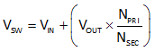
In addition, any leakage inductance of the transformer causes a turnoff voltage spike in addition to Equation 10. This voltage spike is related to the MOSFET drain-to-source capacitance as well as other parasitic capacitances. To limit the spike magnitude, use a RCD termination or a Diode-Zener clamp.