SNVS496F January 2007 – May 2021 LM5002
PRODUCTION DATA
- 1 Features
- 2 Applications
- 3 Description
- 4 Revision History
- 5 Pin Configuration and Functions
- 6 Specifications
- 7 Detailed Description
- 8 Application and Implementation
- 9 Power Supply Recommendations
- 10Layout
- 11Device and Documentation Support
- 12Mechanical, Packaging, and Orderable Information
Package Options
Mechanical Data (Package|Pins)
Thermal pad, mechanical data (Package|Pins)
Orderable Information
8.2.1.2.2 Flyback Transformer
Two things require consideration when specifying a flyback transformer. First, the turns ratio to determine the duty cyle D (MOSFET on-time compared to the switching period). Second, the primary inductance (LPRI) to determine the current sense ramp for current-mode control.
To start, the primary inductance in continous current mode (CCM) is designed to provide a ramp during the MOSFET on-time of around 30% of the full load MOSFET current. This produces a good signal-to-noise ratio for current mode control.
The transfer function of a flyback power stage is Equation 4.
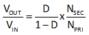
where:
- VIN is the input voltage
- VOUT is the secondary output voltage
- D is the duty cycle of the MOSFET for one switching cycle
- NPRI is the number of turns on the primary winding of the transformer
- NSEC is the number of turns on the secondary winding of the transformer
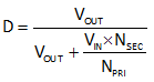
The duty cycle can be derived as shown in Equation 5.
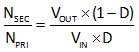
And the approximate turns ratio is given by Equation 6.
The primary inducance (LPRI) is calculated using Equation 7.
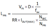
where:
- LPRI is the transformer inductance referenced to the primary side
- RR is the ripple ratio of the reflected secondary output current (ypically between 30% and 40%)
The auxillary winding turns ratio can be found with Equation 8.
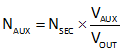
where:
- NAUX is the number of turns on the auxiliary winding of the transformer
- VAUX is the desired VCC voltage
The CCM duty cycle can be designed for 50% with minimum input voltage. Using Equation 6, the turns ratio of the secondary winding to the primay winding can be found to be 0.313. Rounding to a whole number of turns results in a turns ratio of 0.375. The auxillary winding of the transformer can be used to supply the VCC voltage to the LM5002, resulting in better total efficiency by disabling the internal high voltage VCC regulator. To disable the VCC regulator the exteranlly supplied voltage must be greater than 7 V, thus a target voltage of 8 V is selected. The number of turns on the auxillary winding can be found with Equation 8, resulting in a turns ratio of the auxillary winding to the secondary winding of 0.6.
The primary inductance can now be solved for using Equation 7. Assuming that VIN is at the minimum specified value and the ripple ratio (RR) is 35% the primary inductance is calculated to be 217 µH. Based on avaliable transformers a 300 µH primary inductance was selected.