SNVS532D October 2007 – August 2020 LM5067
PRODUCTION DATA
- 1 Features
- 2 Applications
- 3 Description
- 4 Revision History
- 5 Device Comparison
- 6 Pin Configuration and Functions
- 7 Specifications
- 8 Detailed Description
-
9 Application and Implementation
- 9.1 Application Information
- 9.2
Typical Application
- 9.2.1 Design Requirements
- 9.2.2 Detailed Design Procedure
- 9.2.3 Application Curves
- 10Power Supply Recommendations
- 11Layout
- 12Device and Documentation Support
- 13Mechanical, Packaging, and Orderable Information
Package Options
Mechanical Data (Package|Pins)
Thermal pad, mechanical data (Package|Pins)
Orderable Information
8.3.6 Fault Timer and Restart
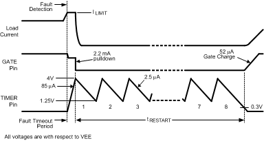
When the current limit or power limit threshold is reached during turn-on or as a result of a fault condition, the gate-to-source voltage of Q1 is modulated to regulate the load current and power dissipation in Q1. When either limiting function is active, an 85 µA fault timer current source charges the external capacitor (CT) at the TIMER pin as shown in Figure 8-5 (Fault Timeout Period). If the fault condition subsides before the TIMER pin reaches 4.0V, the LM5067 returns to the normal operating mode and CT is discharged by the 2.5 µA current sink. If the TIMER pin reaches 4.0V during the Fault Timeout Period, Q1 is switched off by a 2.2 mA pull-down current at the GATE pin. The subsequent restart procedure depends on which version of the LM5067 is in use.
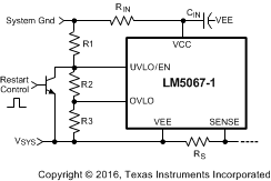
The LM5067-1 latches the GATE pin low at the end of the Fault Timeout Period, and CT is discharged by the 2.5 µA fault current sink. The GATE pin is held low until a power up sequence is externally initiated by cycling the input voltage (VSYS), or momentarily pulling the UVLO/EN pin within 2.5V of VEE with an open-collector or open-drain device as shown in Figure 8-4. The voltage across CT must be <0.3V for the restart procedure to be effective.
 Figure 8-4 Latched Fault Restart Control
The LM5067-2 provides an automatic restart sequence which consists of the TIMER pin cycling between 4 V and 1.25 V seven times after the Fault Timeout Period, as shown in Figure 8-5. The period of each cycle is determined by the 85 µA charging current, and the 2.5 µA discharge current, and the value of the capacitor CT. When the TIMER pin reaches 0.3 V during the eighth high-to-low ramp, the 52 µA current source at the GATE pin turns on Q1. If the fault condition is still present, the Fault Timeout Period and the restart cycle repeat.
 Figure 8-5 Restart Sequence (LM5067-2)